


LOW VOLTAGE DETECTOR
NO. EA-056-0305
R3111xxxxA/C SERIES
OUTLINE
The R3111 series are CMOS-based voltage detector ICs with high detector threshold accuracy and ultra-low supply
current, which can be operated at an extremely low voltage and is used for system reset as an example.
Each of these ICs consists of a voltage reference unit, a comparator, resistors for detector threshold setting, an
output driver and a hysteresis circuit. The detector threshold is fixed with high accuracy internally and does not re-
quire any adjustment.
Two output types, Nch open drain type and CMOS type are available.
The R3111 Series are operable at a lower voltage than that for the RX5VL series, and can be driven by a single
battery.
Five types of packages, TO-92, SOT-89, SOT-23-3, SOT-23-5 and SC-82AB are available.
FEATURES
• Ultra-low Supply Current............................................................ Typ. 0.8µA (V
• Wide Range of Operating Voltage............................................... 0.7V to 10.0V (Topt=25°C)
• Detector Threshold..................................................................... Stepwise setting with a step of 0.1V in the range of
0.9V to 6.0V is possible.
• High Accuracy Detector Threshold............................................ ±2.0%
• Low Temperature-Drift Coefficient of Detector Threshold...... Typ. ±100ppm/°C
• Two Output Types ....................................................................... Nch Open Drain and CMOS
• Four Types of Packages............................................................... TO-92, SOT-89(Mini-power Mold), SOT-23-3,
SOT-23-5 (Mini-mold), SC-82AB
DD
=1.5V)
APPLICATIONS
• CPU and Logic Circuit Reset
• Battery Checker
• Window Comparator
• Wave S h aping Circuit
• Battery Back-up Circuit
• Power Failure Detector
1

R3111xxxxA/C
BLOCK DIAGRAMS
R3111xxxxA R3111xxxxC
V
DD
OUT
V
DD
OUT
Vref
Vref
GND
TIMING CHART
DET
SS
VSS
Detector Threshold
Hysteresis
t
PLH
Supply Voltage
(VDD)
Output Voltage
(OUT)
Release Voltage +V
Detector Threshold -VDET
Minimum Operating Voltage
V
DEFINITION OF OUTPUT DELAY TIME
Output Delay Time t
1. In the case of Nch Open Drain Output:
Under the condition of the output pin (OUT) is pulled up through a resistor of 470kΩ to 5V, the time interval between the rising edge of V
2. In the case of CMOS Output:
The time interval between the rising edge of V
voltage to (V
PLH
is defined as follows:
DD
2) V.
/
+V
DET
+ 2.0V
DD
pulse from 0.7V to (+V
DET
)+ 2.0V and becoming of the output voltage to 2.5V.
DD
pulse from 0.7V to (+V
DET
)+ 2.0V and becoming of the output
+V
DET
+ 2.0V
GND
Input Voltage
DD
)
(V
Output Voltage
0.7V
GND
5.0V
2.5V
GND
t
PHL
t
PLH
Input Voltage
DD
)
(V
Output Voltage
+V
+V
DET
DET
0.7V
GND
+2.0V
+2.0V
2
GND
t
PHL
t
PLH
Nch Open Drain Output CMOS Output
2

R3111xxxxA/C
SELECTION GUIDE
The package type, the detector threshold, the output type and the taping type of R3111 Series can be designated at
the users’ request by specifying the part number as follows;
R3111xxxxx-xx
↑↑↑↑ ↑
abcd e
Code Contents
Designation of Package Type;
a
b
E: TO-92 Q: SC-82AB
H: SOT-89 N: SOT-23-5 / SOT-23-3
Setting Detector Threshold (-V
Stepwise setting with a step of 0.1V in the range of 0.9V to 6.0V is possible.
←
Part Number
DET
);
c
d
e
Designation of Package Type
1: except SOT-23-3 2: SOT-23-3
Designation of Output Type;
A: Nch Open Drain
C: CMOS
Designation of Packing or Taping Type ;
Ex.TO-92: TZ, SOT-89: T1, SOT-23-3, SOT-23-5, SC-82AB: TR prescribed as standard
directions.
(Refer to Taping Specifications.) Antistatic bag for samples: C
3
R3111xxxxA/C
PIN CONFIGURATION
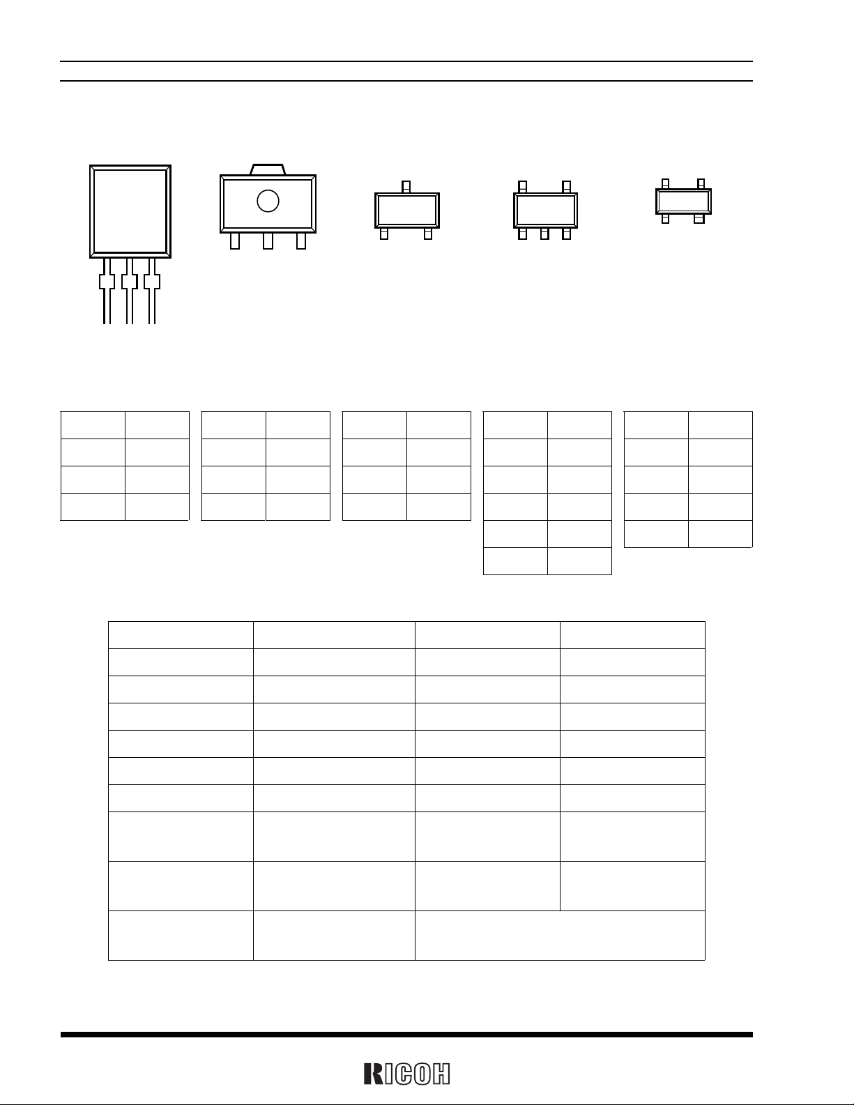
• TO-92 • SOT-89 • SOT-23-3 • SOT-23-5 • SC-82AB
3
54
43
(mark side)
12
(mark side)
123
(mark side)
123
(mark side)
12
(mark side)
123
PIN DESCRIPTION
• TO-92 • SOT-89 • SOT-23-3 • SOT-23-5 • SC-82AB
Pin No. Symbol Pin No. Symbol Pin No. Symbol Pin No. Symbol Pin No. Symbol
1VDD1 OUT 1 OUT 1 OUT 1 OUT
2 GND 2 V
DD
2 GND 2 V
3 OUT 3 GND 3 V
DD
3 GND 3 NC
4 NC 4 GND
5NC
DD
2V
DD
ABSOLUTE MAXIMUM RATINGS
Symbol Item Rating Unit
DD
V
OUT1
V
OUT2
V
OUT
I
D
P
D
P
To p t
Ts t g
Ts o l d e r
*Note 1: applied to SOT-89 and TO-92
*Note 2: applied to SOT-23-3, SOT-23-5 and SC-82AB
Supply Voltage 12 V
Output Voltage (CMOS) VSS-0.3 to VDD+0.3 V
Output Voltage (Nch) VSS-0.3 to 12 V
Output Current 70 mA
Power Dissipation 1*
Power Dissipation 2*
Operating Temperature
Range
Storage Temperature
Range
Lead temperature (Sol-
dering)
Note1
Note2
300 mW
150 mW
-40 to 85 °C
-55 to 125 °C
260°C, 10s
4

R3111xxxxA/C
ELECTRICAL CHARACTERISTICS
• R3111x09xA/C To p t = 2 5 °C
Symbol Item Conditions Min. Typ. Max. Unit
DET
-V
HYS
V
SS
I
DDH
V
DDL
V
OUT
I
PLH
t
Detector Threshold 0.882 0.900 0.918 V
Detector Threshold Hysteresis 0.027 0.045 0.063 V
Supply Current
=0.80V
2.90V
0.8
0.9
2.4
2.7
µA
DD
V
Maximum Operating Voltage 10 V
To p t = 2 5 °C 0.55 0.70
Minimum Operating Voltage*
Note1
-40°C≤To p t ≤85°C 0.65 0.80
Nch
Output Current
V
DS
V
=0.50V,VDD=0.85V
0.01
0.05
0.05
0.50
mA
DS
=0.05V,VDD=0.70V
(Driver Output Pin)
Output Delay Time*
Note2
Pch
V
DS
=-2.1V,VDD=4.5V 1.0 2.0
100 µs
mA
V
∆-V
DET
/∆T
Detector Threshold Temperature
Coefficient
-40°C≤To p t ≤85°C ±100
ppm/°C
• R3111x18xA/C To p t = 2 5 °C
Symbol Item Conditions Min. Typ. Max. U=nit
DET
-V
HYS
V
SS
I
DDH
V
DDL
V
Detector Threshold 1.764 1.800 1.836 V
Detector Threshold Hysteresis 0.054 0.090 0.126 V
Supply Current
=1.70V
3.80V
0.8
1.0
2.4
3.0
µA
DD
V
Maximum Operating Voltage 10 V
To p t = 2 5 °C 0.55 0.70
Minimum Operating Voltage*
Note1
V
-40°C≤To p t ≤85°C 0.65 0.80
Nch
mA
mA
I
t
OUT
PLH
Output Current
(Driver Output Pin)
Output Delay Time*
Note2
DS
=0.05V, VDD=0.70V
V
DS
V
=0.50V, VDD=0.85V
0.01
1.00
Pch
DS
=-2.1V,VDD=4.5V 1.0 2.0
V
0.05
2.00
100 µs
∆-V
DET
/∆T
Detector Threshold Temperature
Coefficient
-40°C≤To p t ≤85°C ±100 ppm/°C
5
R3111xxxxA/C
• R3111x27xA/C To p t = 2 5 °C
Symbol Item Conditions Min. Typ. Max. Unit
DET
-V
HYS
V
SS
I
DDH
V
DDL
V
OUT
I
PLH
t
Detector Threshold 2.646 2.700 2.754 V
Detector Threshold Hysteresis 0.081 0.135 0.189 V
Supply Current
V
=2.60V
4.70V
0.9
1.1
2.7
3.3
µA
DD
Maximum Operating Voltage 10 V
To p t = 2 5 °C 0.55 0.70
Minimum Operating Voltage*
Note1
-40°C≤To p t ≤85°C 0.65 0.80
Nch
Output Current
DS
V
=0.05V,VDD=0.70V
DS
=0.50V,VDD=1.50V
V
0.01
1.00
0.05
2.00
mA
(Driver Output Pin)
Output Delay Time*
Note2
Pch
V
DS
=-2.1V,VDD=4.5V 1.0 2.0
100 µs
mA
V
∆-V
DET
/∆T
Detector Threshold Temperature
-40°C≤To p t ≤85°C ±100 ppm/°C
Coefficient
• R3111x36xA/C To p t = 2 5 °C
Symbol Item Conditions Min. Typ. Max. Unit
DET
-V
HYS
V
SS
I
DDH
V
Detector Threshold 3.528 3.600 3.672 V
Detector Threshold Hysteresis 0.108 0.180 0.252 V
Supply Current
V
=3.47V
5.60V
1.0
1.2
3.0
3.6
µA
DD
Maximum Operating Voltage 10 V
To p t = 2 5 °C 0.55 0.70
DDL
V
Minimum Operating Voltage*
Note1
V
-40°C≤To p t ≤85°C 0.65 0.80
Nch
mA
I
OUT
Output Current
DS
V
=0.05V,VDD=0.70V
DS
V
=0.50V,VDD=1.50V
0.01
1.00
0.05
2.00
(Driver Output Pin)
t
PLH
Output Delay Time*
Note2
Pch
DS
=-2.1V,VDD=4.5V 1.0 2.0
V
100 µs
mA
∆-V
DET
/∆T
Detector Threshold Temperature
-40°C≤To p t ≤85°C ±100 ppm/°C
Coefficient
6

R3111xxxxA/C
• R3111x45xA/C To p t = 2 5 °C
Symbol Item Conditions Min. Typ. Max. Unit
DET
-V
HYS
V
SS
I
DDH
V
DDL
V
OUT
I
PLH
t
Detector Threshold 4.410 4.500 4.590 V
Detector Threshold Hysteresis 0.135 0.225 0.315 V
Supply Current
=4.34V
6.50V
1.1
1.3
3.3
3.9
µA
DD
V
Maximum Operating Voltage 10 V
To p t = 2 5 °C 0.55 0.70
Minimum Operating Voltage*
Note1
-40°C≤To p t ≤85°C 0.65 0.80
Nch
Output Current
V
DS
V
=0.50V, VDD=1.50V
0.01
1.00
0.05
2.00
mA
DS
=0.05V, VDD=0.70V
(Driver Output Pin)
Output Delay Time*
Note2
Pch
V
DS
=-2.1V,VDD=8.0V 1.5 3.0
100 µs
mA
V
∆-V
DET
/∆T
Detector Threshold Temperature
Coefficient
-40°C≤To p t ≤85°C ±100 ppm/°C
• R3111x54xA/C To p t = 2 5 °C
Symbol Item Conditions Min. Typ. Max. Unit
DET
-V
HYS
V
SS
I
DDH
V
DDL
V
Detector Threshold 5.292 5.400 5.508 V
Detector Threshold Hysteresis 0.162 0.270 0.378 V
Supply Current
=5.20V
7.40V
1.2
1.4
3.6
4.2
µA
DD
V
Maximum Operating Voltage 10 V
To p t = 2 5 °C 0.55 0.70
Minimum Operating Voltage*
Note1
V
-40°C≤To p t ≤85°C 0.65 0.80
Nch
DS
V
∆-V
I
t
DET
OUT
PLH
/∆T
Output Current
(Driver Output Pin)
Output Delay Time*
Note2
Detector Threshold Temperature
Coefficient
=0.05V, VDD=0.70V
DS
V
=0.50V, VDD=1.50V
Pch
DS
=-2.1V, VDD=8.0V 1.5 3.0
V
-40°C≤To p t ≤85°C ±100 ppm/°C
0.01
1.00
0.05
2.00
mA
mA
100 µs
*Note1: Minimum operating voltage means the value of input voltage when output voltage maintains 0.1V or
less. (In the case of Nch Open Drain Output type, the output pin is pulled up with a resistance of
470kΩ to 5.0V.)
*Note2: In the case of CMOS Output type: The time interval between the rising edge of VDD input pulse from
0.7V to (+V
)+2.0V and output voltage level becoming to VDD/2.
DET
In the case of Nch Open Drain Output type: the output pin is pulled up with a resistance of 470kΩ to
5.0V, The time interval between the rising edge of VDD input pulse from 0.7V to (+VDET)+2.0V and output voltage level becoming to 2.5V.
7

R3111xxxxA/C
ELECTRICAL CHARACTERISTICS BY DETECTOR THRESHOLD
• R3111x09x to R3111x60x
Part
Number
Detector Threshold
-V
[V] V
DET
Min. Typ. Max. Min. Typ. Max. Condition Typ. Max. Condition Typ. Max.
R3111x09xx 0.882 0.900 0.918 0.027 0.045 0.063
R3111x10xx 0.980 1.000 1.020 0.030 0.050 0.070
R3111x11xx 1.078 1.100 1.122 0.033 0.055 0.077
R3111x12xx 1.176 1.200 1.224 0.036 0.060 0.084
R3111x13xx 1.274 1.300 1.326 0.039 0.065 0.091
R3111x14xx 1.372 1.400 1.428 0.042 0.070 0.098
R3111x15xx 1.470 1.500 1.530 0.045 0.075 0.105
R3111x16xx 1.568 1.600 1.632 0.048 0.080 0.112
R3111x17xx 1.666 1.700 1.734 0.051 0.085 0.119
R3111x18xx 1.764 1.800 1.836 0.054 0.090 0.126
R3111x19xx 1.862 1.900 1.938 0.057 0.095 0.133
R3111x20xx 1.960 2.000 2.040 0.060 0.100 0.140
R3111x21xx 2.058 2.100 2.142 0.063 0.105 0.147
R3111x22xx 2.156 2.200 2.244 0.066 0.110 0.154
R3111x23xx 2.254 2.300 2.346 0.069 0.115 0.161
R3111x24xx 2.352 2.400 2.448 0.072 0.120 0.168
R3111x25xx 2.450 2.500 2.550 0.075 0.125 0.175
R3111x26xx 2.548 2.600 2.652 0.078 0.130 0.182
R3111x27xx 2.646 2.700 2.754 0.081 0.135 0.189
R3111x28xx 2.744 2.800 2.856 0.084 0.140 0.196
R3111x29xx 2.842 2.900 2.958 0.087 0.145 0.203
R3111x30xx 2.940 3.000 3.060 0.090 0.150 0.210
R3111x31xx 3.038 3.100 3.162 0.093 0.155 0.217
R3111x32xx 3.136 3.200 3.264 0.096 0.160 0.224
R3111x33xx 3.234 3.300 3.366 0.099 0.165 0.231
R3111x34xx 3.332 3.400 3.468 0.102 0.170 0.238
R3111x35xx 3.430 3.500 3.570 0.105 0.175 0.245
R3111x36xx 3.528 3.600 3.672 0.108 0.180 0.252
R3111x37xx 3.626 3.700 3.774 0.111 0.185 0.259
R3111x38xx 3.724 3.800 3.876 0.114 0.190 0.266
R3111x39xx 3.822 3.900 3.978 0.117 0.195 0.273
R3111x40xx 3.920 4.000 4.080 0.120 0.200 0.280
R3111x41xx 4.018 4.100 4.182 0.123 0.205 0.287
R3111x42xx 4.116 4.200 4.284 0.126 0.210 0.294
R3111x43xx 4.214 4.300 4.386 0.129 0.215 0.301
R3111x44xx 4.312 4.400 4.488 0.132 0.220 0.308
R3111x45xx 4.410 4.500 4.590 0.135 0.225 0.315
R3111x46xx 4.508 4.600 4.692 0.138 0.230 0.322
R3111x47xx 4.606 4.700 4.794 0.141 0.235 0.329
R3111x48xx 4.704 4.800 4.896 0.144 0.240 0.336
R3111x49xx 4.802 4.900 4.998 0.147 0.245 0.343
R3111x50xx 4.900 5.000 5.100 0.150 0.250 0.350
R3111x51xx 4.998 5.100 5.202 0.153 0.255 0.357
R3111x52xx 5.096 5.200 5.304 0.156 0.260 0.364
R3111x53xx 5.194 5.300 5.406 0.159 0.265 0.371
R3111x54xx 5.292 5.400 5.508 0.162 0.270 0.378
R3111x55xx 5.390 5.500 5.610 0.165 0.275 0.385
R3111x56xx 5.488 5.600 5.712 0.168 0.280 0.392
R3111x57xx 5.586 5.700 5.814 0.171 0.285 0.399
R3111x58xx 5.684 5.800 5.916 0.174 0.290 0.406
R3111x59xx 5.782 5.900 6.018 0.177 0.295 0.413
R3111x60xx 5.880 6.000 6.120 0.180 0.300 0.420
Note 1: In the case of CMOS output type; when the voltage is forced to VDD from 0.7V to (+V
Note 2: VDD value when Output Voltage is equal or less than 0.1V. In the case of Nch open drain output type, the output pin is pulled
edge of VDD and the reaching point at 50% of Output Voltage. In the case of Nch open drain output type : The output pin is
pulled up to 5V through 470kΩ,and when the voltage is forced to VDD from 0.7V to (+V
ing edge of VDD and the reaching point ar 50% of Output Voltage.
up to 5V through 470kΩ resistor.
Condition 1: Topt=25°C
Condition 2: -40°C≤Topt≤85°C
Detector Threshold
Hysteresis
[V]
HYS
Supply Current 1 Supply Current 2
[µµµµA] I
I
SS1
SS2
[µµµµA]
0.8 2.4
DD
V
=
DET
(-V
)
-0.10V
0.9 2.7 1.1 3.3
DD
V
DET
(-V
-0.13V
DD
V
DET
(-V
=
)
1.0 3.0 1.2 3.6
=
)
1.1 3.3 1.3 3.9
DD
V
DET
(-V
+2.0V
=
)
-0.16V
DD
V
=
DET
)
(-V
1.2 3.6
-0.20V
)+2.0V, time interval between the rising
DET
)+2.0V, time interval between the ris-
DET
0.9 2.7
1.0 3.0
1.4 4.2
8

R3111xxxxA/C
Output Current 1 Output Current 2
I
[mA] I
OUT1
Condition Min. Typ.
Condition
VDD=
0.85V
VDD=
1.0V
Nch
DS
V
0.5V
=
DD
V
DS
V
V
Nch
=0.05V
DD
=0.7V
0.01 0.05
1.5V
OUT2
[mA]
Output Delay
Time
[µµµµs]
t
PLH
Minimum Operat-
ing Voltage
V
[V]
DDL
Detector Threshold Tem-
perature Coefficient
∆∆∆∆-V
DET
Min. Typ. Max. Typ. Max. Condition Typ.
0.05 0.5
0.2 1.0
=
1.0 2.0
Note 1
100
Note 2
Condi-
tion 1
Condi-
tion 2
0.55
0.65
Note 2
Condi-
tion 1
0.70
Condi-
tion 2
0.80
-40°C≤
To p t
≤85°C
/∆∆∆∆T[ppm/°°°°C]
±100
9
R3111xxxxA/C
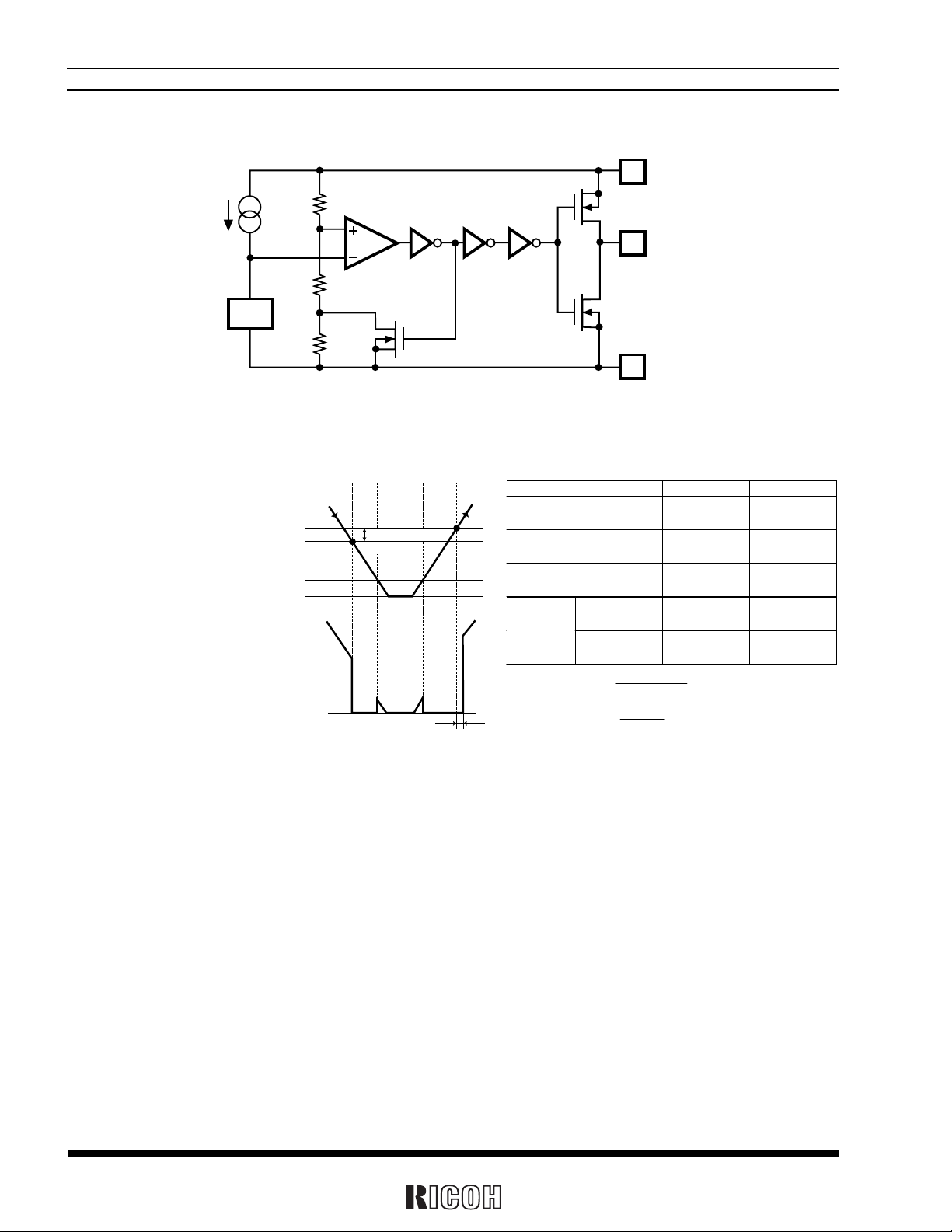
OPERATION
V
DD
Supply Voltage
(VDD)
Output Voltage
(V
OUT)
Vref
Released Voltage(+V
Detector Threshold(-V
Minimum Operating Voltage
GND
GND
DET)
DET)
Ra
Rb
Comparator
Rc
Figure 1. Block Diagram
12 3 4 5
Detector Threshold
Hysteresis
A
Pch
OUT
Nch
GND
Step 12345
B
t
PLH
Comparator
Pin Input Voltage
Comparator Output H L
Tr. 1 OF F O N
Pch ON OFF
Output Tr.
Nch OFF ON
I II III IV V
Indefinite
Indefinite
Indefinite
Indefinite
RcRb
+
I.
II.
Rb
+
V
x
DD
RcRbRa
++
x V
DD
RbRa
LH
ON OFF
OFF ON
ON OFF
10
Figure 2. Operation Diagram
DD
Step 1. The output voltage is equal to the supply voltage (V
DD
×
Step 2. At Point “A”, Vref≥V
(Rb+Rc)/(Ra+Rb+Rc) is true, as a result, the output of comparator is reverse,
).
and output voltage becomes to GND level. The voltage level of Point A means detector threshold volt-
age, or (-V
DET
).
Step 3. When the supply voltage is less than minimum operating voltage, the operation of output transistor be-
comes indefinite, and in the case that output is pulled up to V
DD
, the output voltage equals to VDD volt-
age.
Step 4. The output voltage equals to GND level.
DD
×
Step 5. At Point “B”, Vref≤V
equal to the supply voltage, or (V
Rb/(Ra+Rb) is true, Output of the comparator is reverse, and output voltage is
DD
). The voltage level of Point B means released voltage, or (+V
DET
).
* The difference between released voltage and detector threshold voltage is the detector threshold hysteresis.

TEST CIRCUITS
I
SS
R3111xxxxA/C
5.0V
V
DD
VDD
470k
IN
R3111
V
IN
Series
X
OUT
V
GND
R3111X
Series
OUT
GND
VOUT
Pull-up circuit is not necessary for
CMOS Output type, or R3111XXXXC.
Figure 3. Supply Current Test Circuit Figure 4. Detector Threshold Test Circuit
V
X
GND
DS
OUT
I
OUT
V
DD- VDS
V
V
DD
OUT
OUT
I
IN
V
V
DS
R3111
IN
V
X
Series
DD
R3111
Series
GND
*Apply to CMOS Output type only
Figure 5. Nch Driver Output Current Test
Figure 6. Pch Driver Output Current Test Circuit
Circuit
+VDET+2.0V
0.7V
VSS
P.G.
VDD
R3111XXXXA
Series
GND
OUT
OUT
R
470k
COUT
+5.0V
OUT
+V
DET
+2.0V
0.7V
V
SS
P.G.
R
100k
V
DD
C
IN
R3111
IN
Series
GND
XXXX
A
OUT
VSS
Figure 7. Output Delay Time Test Circuit (1) Figure 8. Output Delay Time Test Circuit (2)
OUT
R
470k
+5.0V
OUT
V
SS
11
R3111xxxxA/C
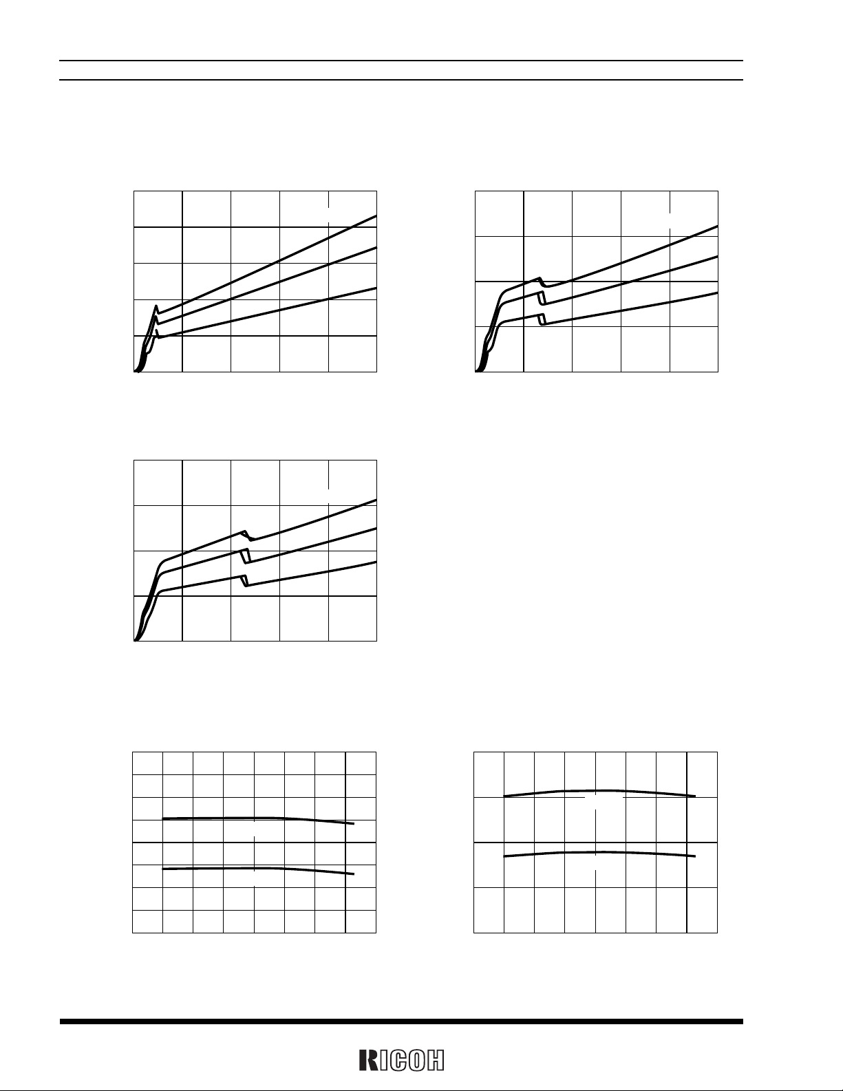
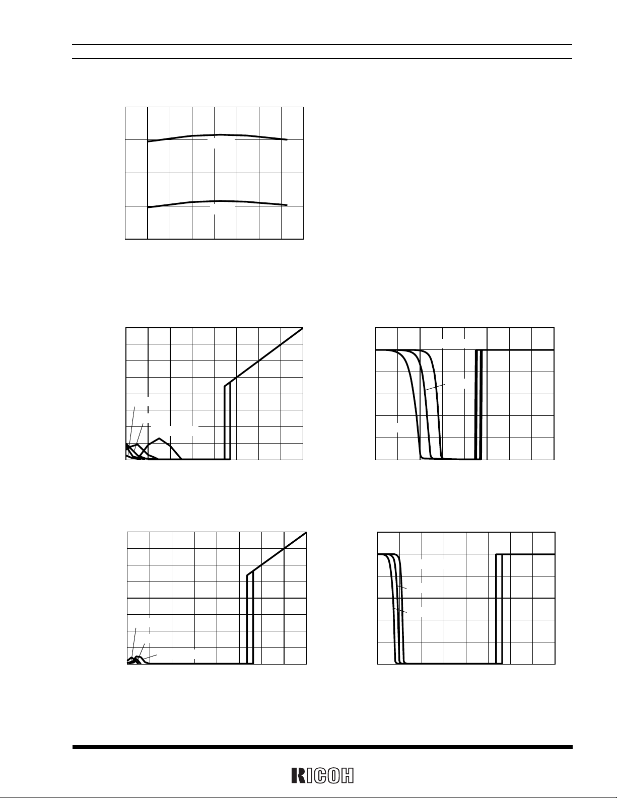
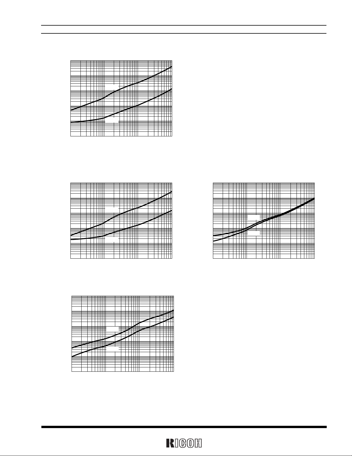
TYPICAL CHARACTERISTICS
1) Supply Current vs. Input Voltage
R3111x09xC R3111x27xC
2.5
2.0
2.0
(µA)
SS
1.5
1.0
0.5
Supply Current I
0.0
0246810
Input Voltage V
Topt=85°C
IN
(V)
25°C
-40°C
R3111x45xC
2.0
1.5
(µA)
SS
1.0
0.5
Supply Current I
Topt=85°C
-40°C
25°C
Topt=85°C
1.5
(µA)
SS
1.0
-40°C
0.5
Supply Current I
0.0
0246810
IN
Input Voltage V
(V)
25°C
0.0
0246810
IN
Input Voltage V
(V)
2) Detector Threshold Hysteresis vs. Temperature
R3111x09xC R3111x27xC
1.00
0.98
0.96
0.94
0.92
0.90
0.88
0.86
Detector Threshold -VDET(V)
0.84
-60 0 20406080-40 -20 100
Temperature Topt(°C)
+VDET
-VDET
2.9
2.8
2.7
2.6
+VDET
-VDET
Detector Threshold -VDET(V)
2.5
-60 0 20406080-40 -20 100
Temperature Topt(°C)
12
4.8
R3111xxxxA/C
R3111x45xC
4.7
+VDET
4.6
4.5
-VDET
Detector Threshold -VDET(V)
4.4
-60 0 20406080-40 -20 100
Temperature Topt(°C)
3) Output Voltage vs. Input Voltage
R3111x09xA R3111x09xA
1.6
1.4
1.2
1.0
0.8
85°C
0.6
25°C
Output Voltage VOUT(V)
0.4
0.2
Topt=-40°C
0.0
0 0.6 0.8 1 1.2 1.40.2 0.4 1.6
Input Voltage V
V
DD Pull-up 470kΩ
IN(V)
6
5
Topt=-40°C
5V Pull-up 470kΩ
4
25°C
3
2
85°C
Output Voltage VOUT(V)
1
0
0 0.6 0.8 1 1.2 1.40.2 0.4 1.6
Input Voltage V
IN(V)
4.0
3.5
(V)
3.0
OUT
2.5
2.0
1.5
1.0
Output Voltage V
0.5
0.0
R3111x27xA R3111x27xA
VDD Pull-up 470kΩ
85°C
25°C
Topt=-40°C
0 1.5 2 2.5 3 3.50.5 1 4
IN
Input Voltage V
(V)
6
5
(V)
OUT
4
3
2
Output Voltage V
1
0
5V Pull-up 470kΩ
Topt=-40°C
25°C
85°C
0 1.5 2 2.5 3 3.50.5 1 4
Input Voltage V
IN
(V)
13

R3111xxxxA/C
R3111x45xA R3111x45xA
6
5
4
3
85°C
2
Output Voltage VOUT(V)
25°C
1
Topt=-40°C
0
0231654
Input Voltage V
4) Nch Driver Output Current vs. VDS
R3111x09xC R3111x09xC
700
VDD Pull-up 470kΩ
IN(V)
Topt=25°C
6
Topt=-40°C
5
25°C
4
85°C
3
2
Output Voltage VOUT(V)
1
0
0231654
Input Voltage V
300
5V Pull-up 470kΩ
IN(V)
Topt=25°C
600
DD=0.85V
V
500
400
300
Output Current IOUT(µA)
200
100
0.7V
0
0 0.2 0.4 0.6 0.8
V
DS(V)
R3111x27xC R3111x27xC
20
18
16
14
12
10
8
6
4
Output Current IOUT(mA)
2
0
0 0.5 1 1.5 2 2.5
V
1.5V
DS(V)
Topt=25°C
VDD=2.5V
2.0V
250
VDD=0.8V
200
150
Output Current IOUT(µA)
100
50
0.7V
0
0 0.02 0.04 0.06 0.08 0.1
V
DS(V)
300
250
VDD=0.8V
200
150
0.7V
Output Current IOUT(µA)
100
50
0
0 0.02 0.04 0.06 0.08 0.1
V
DS(V)
Topt=25°C
14

60
R3111x45xC R3111x45xC
Topt=25°C
300
R3111xxxxA/C
Topt=25°C
50
VDD=4.5V
40
3.5V
Output Current IOUT(mA)
30
20
10
2.0V
3.0V
2.5V
1.5V
0
0 0.5 1 1.5 2 2.5 3 43.5 4.5
V
DS(V)
5) Nch Driver Output Current vs. Input Voltage
R3111x09xC R3111x27xC
900
800
700
(mA)
600
OUT
500
400
300
200
Output Current I
100
0
0 0.2 0.4 0.6 10.8
Input Voltage V
Topt=-85°C
25°C
IN
-40°C
(V)
4.0V
250
VDD=0.8V
200
150
0.7V
100
Output Current IOUT(µA)
50
0
0 0.02 0.04 0.06 0.08 0.1
V
DS(V)
14
12
(mA)
10
OUT
Topt=-40°C
8
6
4
Output Current I
2
0
0 0.5 1 1.5 1 2.5 3
IN
Input Voltage V
(V)
25°C
85°C
R3111x45xC
25
20
(mA)
OUT
15
10
5
Output Current I
0
0123456
Topt=-40°C
25°C
85°C
Input Voltage V
IN
(V)
15

R3111xxxxA/C
6) Pch Driver Output Current vs. Input Voltage
R3111x09xC R3111x27xC
1.4
Topt=25°C
3.5
Topt=25°C
1.2
VDS=0.7V
1.0
0.8
0.6
0.5V
0.4
Output Current IOUT(mA)
0.2
0.0
02468
Input Voltage V
IN(V)
R3111x45xC
IN
(V)
Topt=25°C
1.5V
1.0V
0.5V
4.5
4.0
(mA)
OUT
3.5
3.0
VDS=2.1V
2.5
2.0
1.5
1.0
Output Current I
0.5
0.0
024 8610
Input Voltage V
3.0
2.5
VDS=2.1V
2.0
1.5V
1.5
1.0V
0.5V
Output Current IOUT(mA)
1.0
0.5
0.0
012 43657
Input Voltage V
IN(V)
7) Output Delay Time vs. Load Capacitance
R3111x09xA R3111x27xA
100
10
1
tPLH
0.1
0.01
tPHL
Output Delay Time tP(ms)
0.001
0.0001 0.010.001 0.1
Load Capacitance C
16
OUT
(µF)
100
10
1
tPLH
0.1
0.01
tPHL
Output Delay Time tP(ms)
0.001
0.0001 0.010.001 0.1
Load Capacitance C
OUT
(µF)
R3111x45xA
100
10
t
1
PLH
0.1
t
0.01
PHL
Output Delay Time tP(ms)
0.001
0.0001 0.010.001 0.1
OUT
Load Capacitance C
(µF)
8) Output Delay Time vs. Input Pin Capacitance
R3111x09xA R3111x27xA
100
R3111xxxxA/C
100
10
t
1
PLH
0.1
t
0.01
PHL
Output Delay Time tP(ms)
0.001
0.0001 0.010.001 0.1
IN
Input Pin Capacitance C
(µF)
R3111x45xA
100
10
1
0.1
0.01
Output Delay Time tP(ms)
0.001
0.001 0.10.01 1
t
PLH
t
PHL
Input Pin Capacitance C
IN
(µF)
10
1
t
PLH
0.1
t
PHL
0.01
Output Delay Time tP(ms)
0.001
0.0001 0.010.001 0.1
Input Load Capacitance C
IN
(µF)
17
R3111xxxxA/C
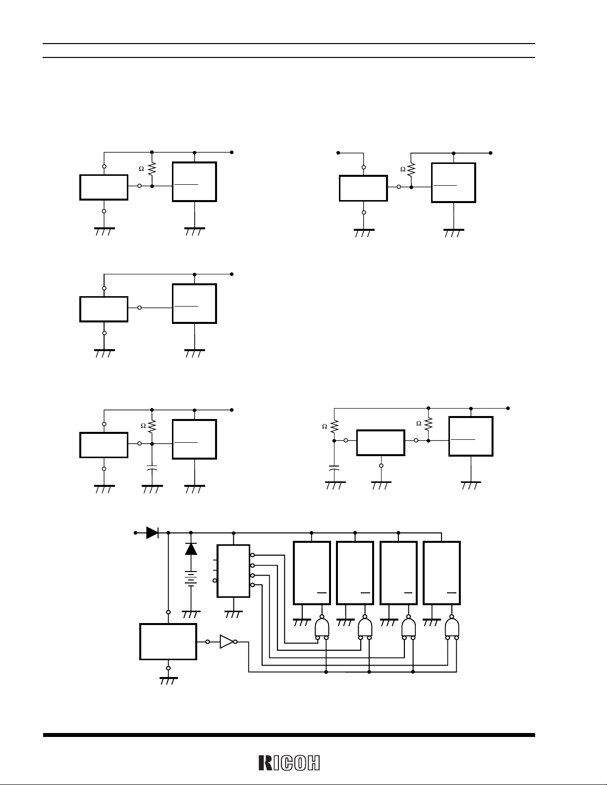
TYPICAL APPLICATION
• R3111xxxxA CPU Reset Circuit (Nch Open Drain Output)
Case 1.Input Voltage to R3111xxxxA is equal to In-
put Voltage to CPU
V
DD
V
DD
R3111
SERIES
GND
XXXX
470k
A
OUT
R
V
RESET
GND
DD
CPU
Case 2.Input Voltage to R3111xxxxA is unequal to
Input Voltage to CPU
V
DD1
V
DD
R3111
SERIES
GND
XXXX
470k
A
OUT
R
V
RESET
GND
DD
CPU
V
DD2
• R3111xxxxA CPU Reset Circuit CMOS Output
V
DD
V
DD
R3111
SERIES
GND
XXXX
C
OUT
V
RESET
GND
DD
CPU
• R3111xxxxA Output Delay Time Circuit 1
(Nch Open Drain Output)
V
DD
V
DD
R3111
SERIES
GND
XXXX
470k
A
OUT
R
V
RESET
GND
DD
CPU
• Memory Back-up Circuit
V
DD
D1
D2
V
DD
A
B
G
GND
V
Y1
Y2
Y3
Y4
CC
• R3111xxxxA Output Delay Time Circuit 2
(Nch Open Drain Output)
R2R1
VCC
VDD
RESET
GND
CPU
XXXX
470k
A
OUT
VCC
100k
CC
V
R3111
SERIES
V
DD
GND
VCC
RAM1 RAM2 RAM3 RAM4
GND CS
GND CS
GND CS
GND CS
DD
V
18
R3111
SERIES
GND
XXX
XC
OUT

• Voltage level Indicator Circuit (lighted when the power runs out)
(Nch Open Drain Output)
V
DD
V
DD
R3111
XXXX
A
SERIES
OUT
GND
• Detector Threshold Adjustable Circuit
(Nch Open Drain Output)
V
OUT
R3111
SERIES
GND
XXXX
DD
Ra
V
DD
A
+
C
Rb
Adjusted Detector Threshold
=(-V
DET)*(Ra+Rb)/Rb
Hysteresis Voltage
=(V
HYS)*(Ra+Rb)/Rb
R3111xxxxA/C
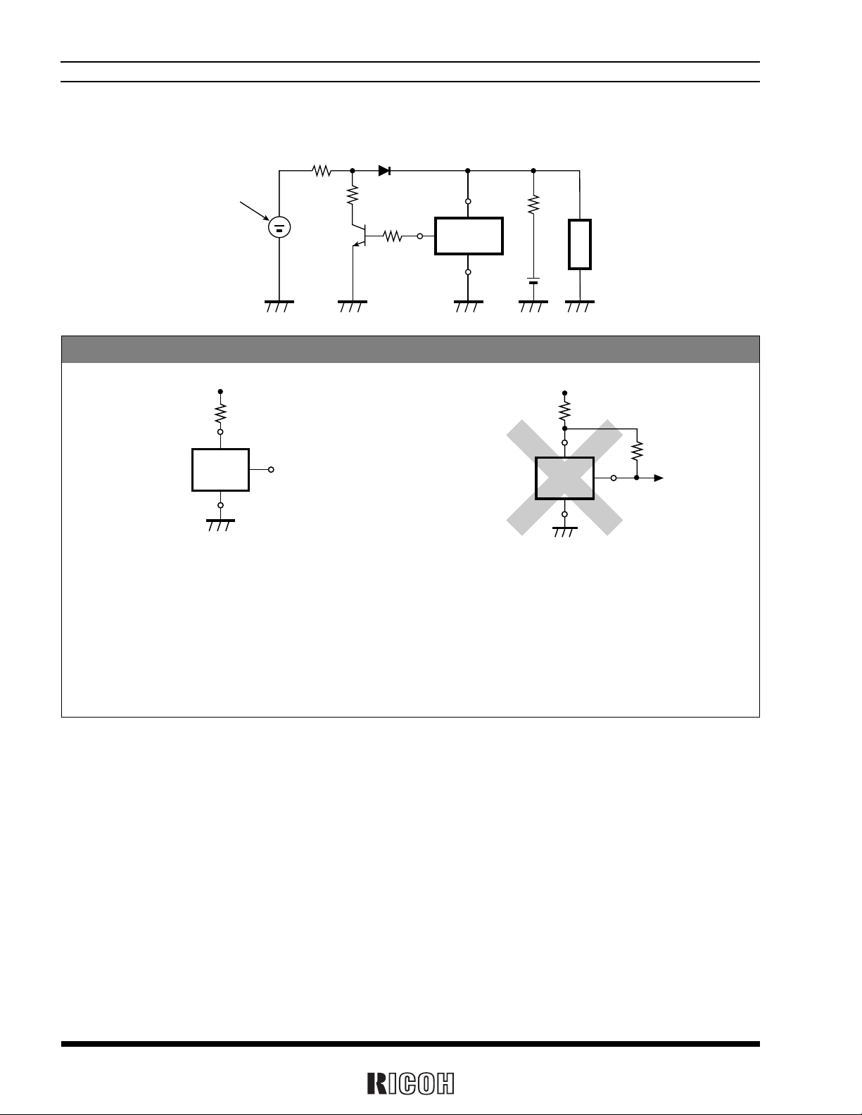
• Window Comparator Circuit
(Nch Open Drain Output)
V
DD
R3111
V
DD
R3111
SERIES
GND
XXXX
OUT
A
V
DET
1
SERIES
GND
XXXX
*) If the value of Ra is set excessively large, voltage drop may
occur caused by the supply current of IC itself, and detector
threshold may vary.
V
DD
OUT
A
V
DET
OUT
2
V
DD
V
SS
DET
1
V
V
DET
2
OUT
V
SS
19
R3111xxxxA/C
• Over-charge Preventing Circuit
Light
R1
Solar Battery
R2
D1
R3
OUT
VDD
R3111
SERIES
GND
R4
XXXXC
TECHNICAL NOTES
V
V
DD
V
DD
R3111
SERIES
GND
R
OUT
DD
V
DD
R3111
SERIES
GND
Figure 9 Figure 10
Load
R1
R2
OUT
1. In Figure 9, When R3111xxxxC is used, and if an impedance is connected between Voltage Supplier and the V
Pin of R3111xxxxC Series, the operation might be unstable by cross conduction current at detection.
When R3111xxxxA is used in Figure 9, if the value of R is set excessively large, voltage drop may occur caused
by supply crrent of IC itself and Detector threshold may vary.
2. Wiring as shown in Figure 10 may cause the oscillation in both output types of R3111 Series.
DD
20
 Loading...