查询ST300S08P1供应商
PHASE CONTROL THYRISTORS Stud V ersion
Bulletin I25158 rev. B 01/94
ST300S SERIES
Features
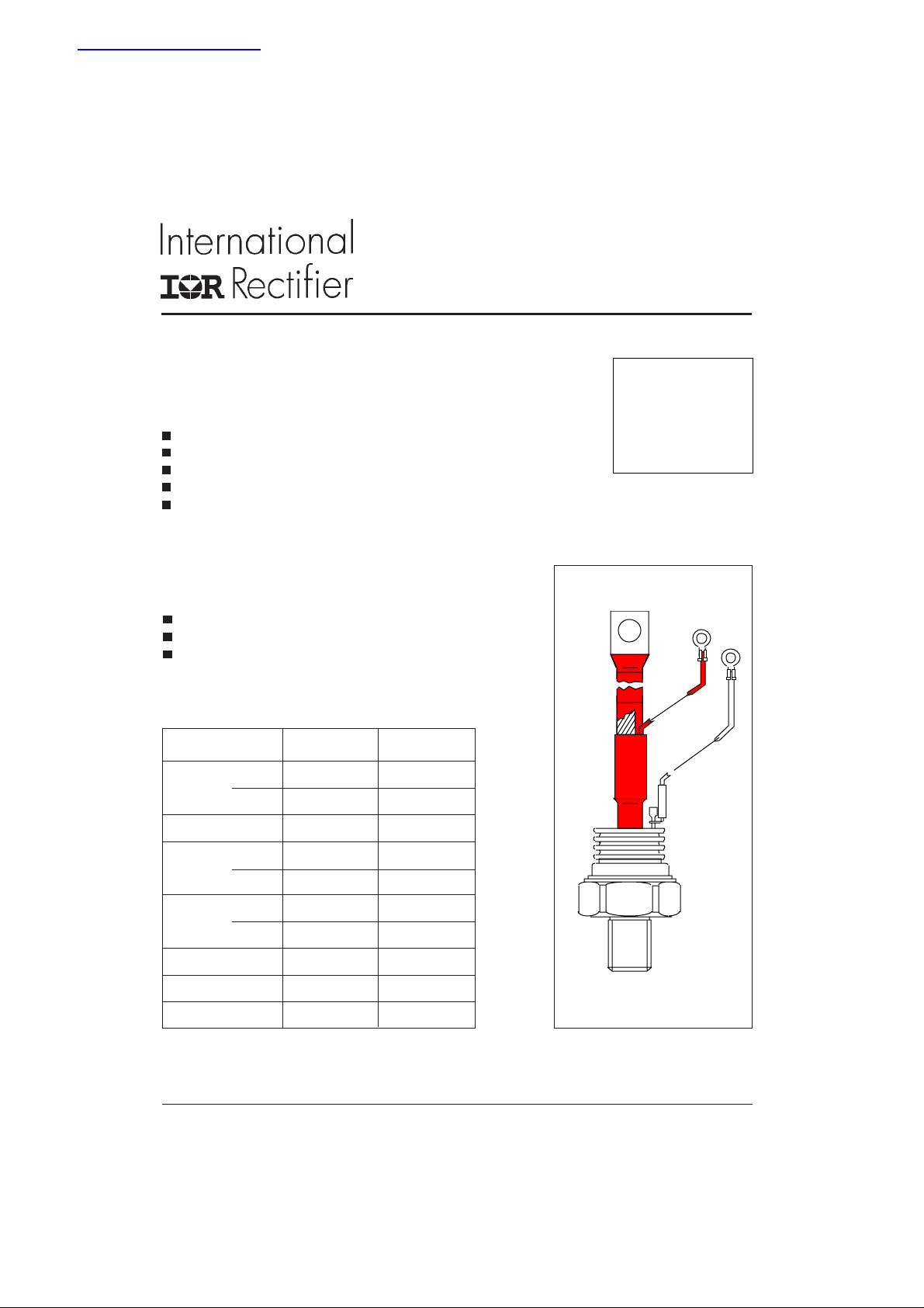
Center amplifying gate
Hermetic metal case with ceramic insulator
International standard case TO-209AE (TO-118)
Threaded studs UNF 3/4 - 16UNF2A or ISO M24x1.5
Compression Bonded Encapsulation for heavy duty
operations such as severe thermal cycling
Typical Applications
DC motor controls
Controlled DC power supplies
AC controllers
Major Ratings and Characteristics
Parameters ST300S Units
I
T(AV)
I
T(RMS)
I
TSM
@ T
C
@ 50Hz 8000 A
@ 60Hz 8380 A
300 A
75 °C
470 A
300A
I2t@
V
DRM/VRRM
t
q
T
J
50Hz 320 KA2s
@ 60Hz 292 KA
typical 100 µs
www.irf.com
400 to 2000 V
- 40 to 125 °C
2
s
case style
TO-209AE (TO-118)
1

ST300S Series
Bulletin I25158 rev. B 01/94
ELECTRICAL SPECIFICATIONS
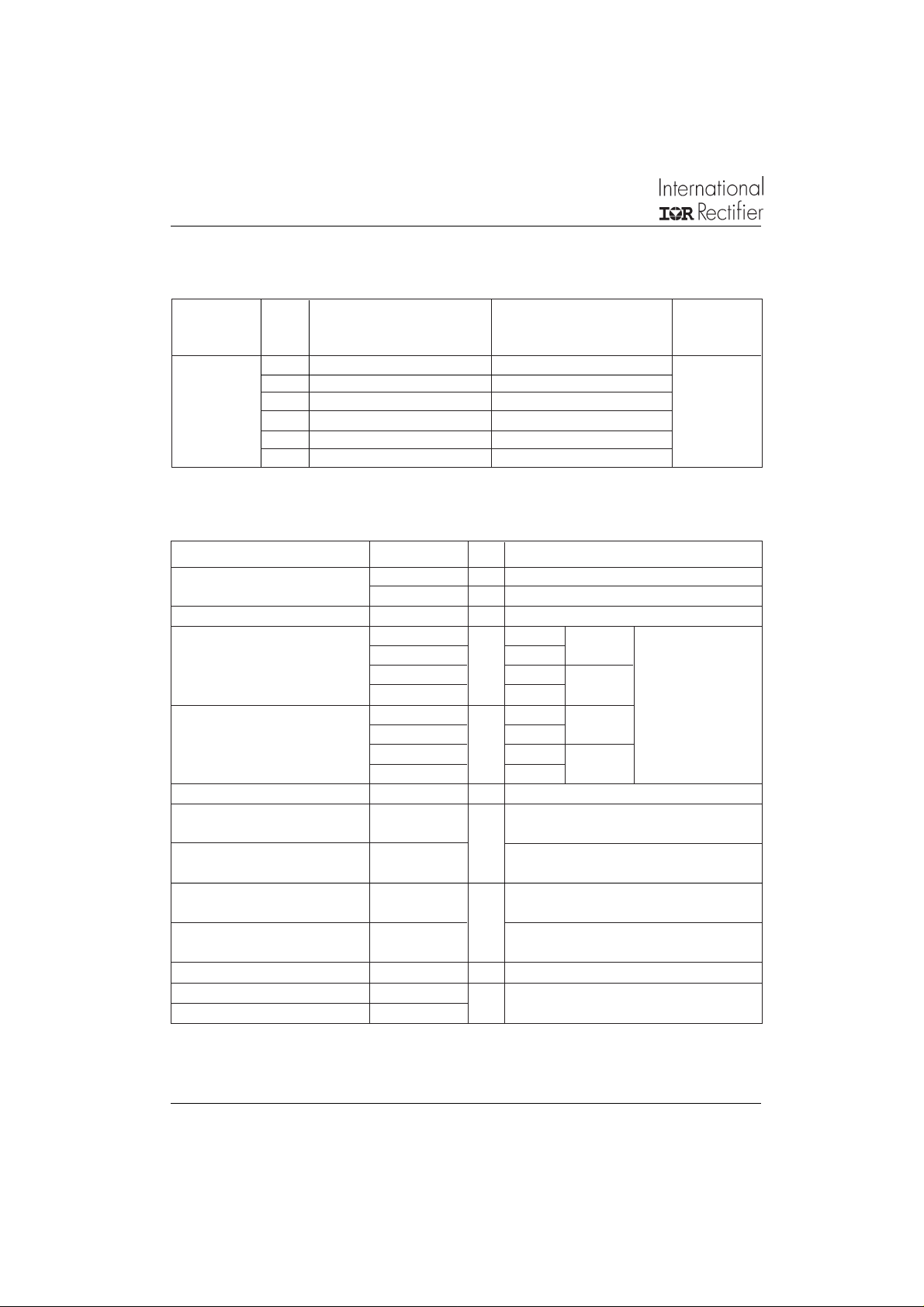
Voltage Ratings
Voltage V
DRM/VRRM
Type number Code peak and off-state voltage repetitive peak voltage @ T
04 400 500
08 800 900
ST300S 50
12 1200 1300
16 1600 1700
18 1800 1900
20 2000 2100
On-state Conduction
Parameter ST300S Units Conditions
I
Max. average on-state current 300 A 180° conduction, half sine wave
T(AV)
@ Case temperature 75 ° C
I
Max. RMS on-state current 470 A DC @ 64°C case temperature
T(RMS)
I
Max. peak, one-cycle 8000 t = 10ms No voltage
TSM
non-repetitive surge current 8380 t = 8.3ms reapplied
2
t Maximum I2t for fusing 320 t = 10ms No voltage Initial TJ = TJ max.
I
2
I
√t Maximum I2√t for fusing 3200 KA2√s t = 0.1 to 10ms, no voltage reapplied
Low level value of threshold
V
T(TO)1
voltage
High level value of threshold
V
T(TO)2
voltage
r
Low level value of on-state
t1
slope resistance
High level value of on-state
r
t2
slope resistance
V
Max. on-state voltage 1.66 V Ipk= 940A, TJ = TJ max, tp = 10ms sine pulse
TM
I
Maximum holding current 600
H
I
Typical latching current 1000
L
, max. repetitive V
, maximum non- I
RSM
DRM/IRRM
VVmA
6730 t = 10ms 100% V
7040 t = 8.3ms reapplied Sinusoidal half wave,
292 t = 8.3ms reapplied
226 t = 10ms 100% V
207 t = 8.3ms reapplied
0.97 (16.7% x π x I
0.98 (I > π x I
0.74 (16.7% x π x I
0.73 (I > π x I
A
KA2s
V
mΩ
mA T
RRM
RRM
< I < π x I
T(AV)
),TJ = TJ max.
T(AV)
< I < π x I
T(AV)
),TJ = TJ max.
T(AV)
= 2 5 ° C , anode supply 12V resistive load
J
), TJ = TJ max.
T(AV)
), TJ = TJ max.
T(AV)
max.
= TJ max
J
2
www.irf.com

Switching
Parameter ST300S Units Conditions
di/dt Max. non-repetitive rate of rise Gate drive 20V, 20Ω, t
of turned-on current T
t
Typical delay time 1.0
d
Typical turn-off time 10 0
t
q
1000 A/µs
µs
= TJ max, anode voltage ≤ 80% V
J
Gate current 1A, dig/dt = 1A/µs
= 0.67% V
V
d
= 550A, TJ = TJ max, di/dt = 40A/µs, VR = 50V
I
TM
dv/dt
DRM, TJ
= 20V/µs, Gate 0V 100Ω, t
Blocking
Parameter ST300S Units Conditions
dv/dt Maximum critical rate of rise of
off-state voltage
Max. peak reverse and off-state
I
RRM
leakage current
I
DRM
500 V/µs TJ = TJ max. linear to 80% rated V
50 mA TJ = TJ max, rated V
ST300S Series
Bulletin I25158 rev. B 01/94
≤ 1µs
r
DRM
= 25°C
= 500µs
p
DRM
DRM/VRRM
applied
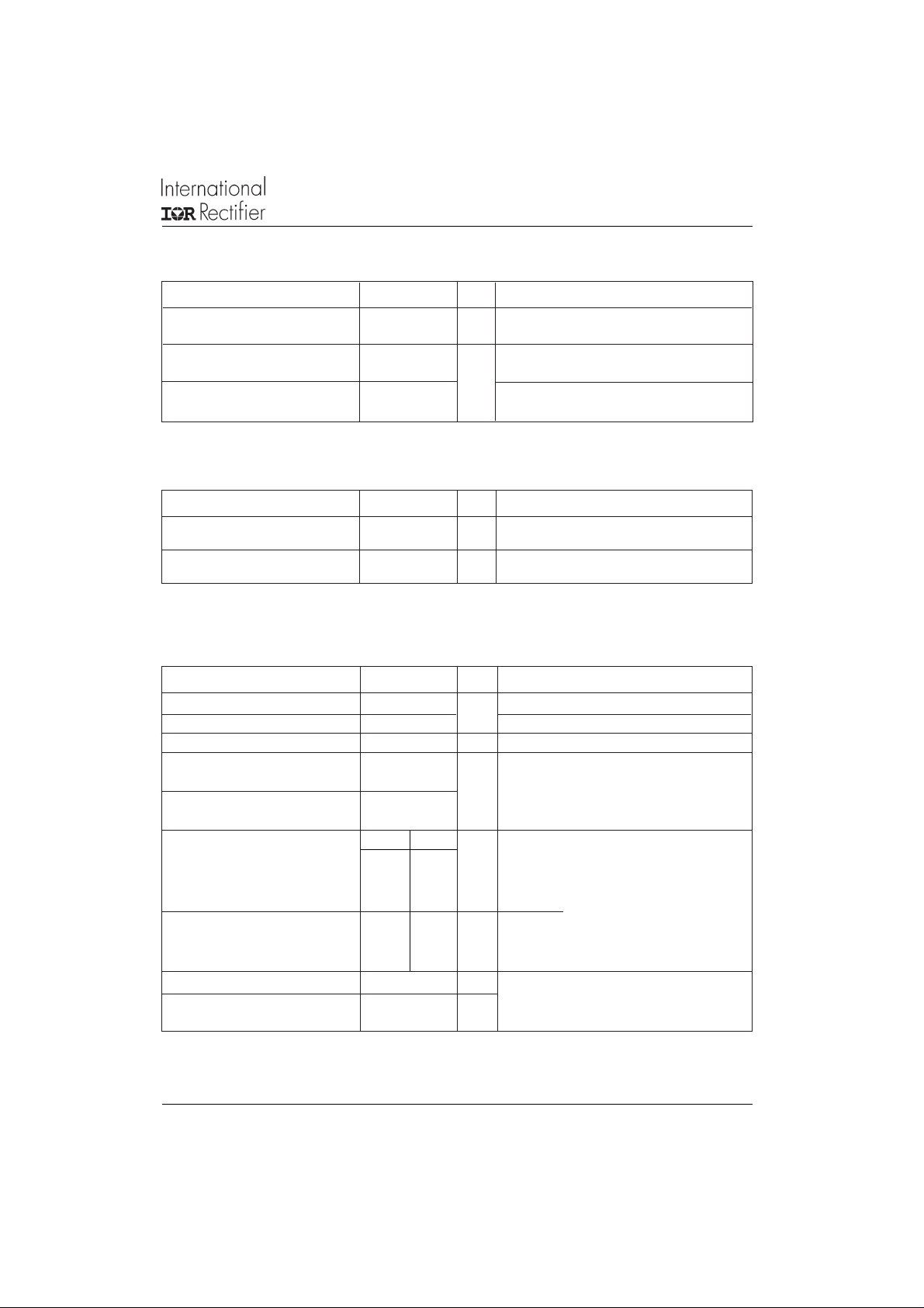
Triggering
Parameter ST300S Units Conditions
PGMMaximum peak gate power 10.0 TJ = TJ max, tp ≤ 5ms
P
Maximum average gate power 2.0 TJ = TJ max, f = 50Hz, d% = 50
G(AV)
I
Max. peak positive gate current 3.0 A TJ = TJ max, tp ≤ 5ms
GM
+V
Maximum peak positive
GM
gate voltage
Maximum peak negative
-V
GM
gate voltage
20
5.0
TYP. MAX.
I
DC gate current required TJ = - 40°C
GT
to trigger mA T
200 100 200
50 -
VGTDC gate voltage required TJ = - 40°C
to trigger V TJ = 25°C
2.5 -
1.8 3
1.1 -
I
DC gate current not to trigger 10.0 mA
GD
VGDDC gate voltage not to trigger 0.25 V
W
VTJ = TJ max, tp ≤ 5ms
= 25°C
J
TJ = 125°C
T
= 125°C
J
T
= TJ max
J
Max. required gate trigger/ current/ voltage are the lowest value
which will trigger all units 12V
anode-to-cathode applied
Max. gate current/ voltage not to
trigger is the max. value which
will not trigger any unit with rated
anode-to-cathode applied
V
DRM
www.irf.com
3
 Loading...