

PD-97657
SupIRBuck
TM
INTEGRATED 12A SYNCHRONOUS BUCK REGULATOR
Features
• Greater than 96% Maximum Efficiency
• Wide Input Voltage Range 1.5V to 16V
• Wide Output Voltage Range 0.7V to 0.9*Vin
• Continuous 12A Load Capability
• Integrated Bootstrap-diode
• High Bandwidth E/A for excellent transient
performance
• Programmable Switching Frequency up to 1.5MHz
• Programmable Over Current Protection
• PGood output
• Hiccup Current Limit
• Precision Reference Voltage (0.7V, +/-1%)
• Programmable Soft-Start
• Enable Input with Voltage Monitoring Capability
• Enhanced Pre-Bias Start-up
• Seq input for Tracking applications
o
• -40
• Thermal Protection
• Pin compatible option for 4A, 8A, and 14A devices
• 5mm x 6mm Power QFN package, 0.9 mm height
• Lead-free, halogen-free and RoHS compliant
C to 125oC operating junction temperature
IR3840WMPbF
HIGHLY EFFICIENT
Description
The IR3840W SupIRBuck
fully integrated and highly efficient DC/DC
synchronous Buck regulator. The MOSFETs copackaged with the on-chip PWM controller make
IR3840W a space-efficient solution, providing
accurate power delivery for low output voltage
applications.
IR3840W is a versatile regulator which offers
programmability of start up time, switching
frequency and current limit while operating in
wide input and output voltage range.
The switching frequency is programmable from
250kHz to 1.5MHz for an optimum solution.
It also features important protection functions,
such as Pre-Bias startup, hiccup current limit and
thermal shutdown to give required system level
security in the event of fault conditions.
TM
is an easy-to-use,
Applications
• Server Applications
• Storage Applications
• Embedded Telecom Systems
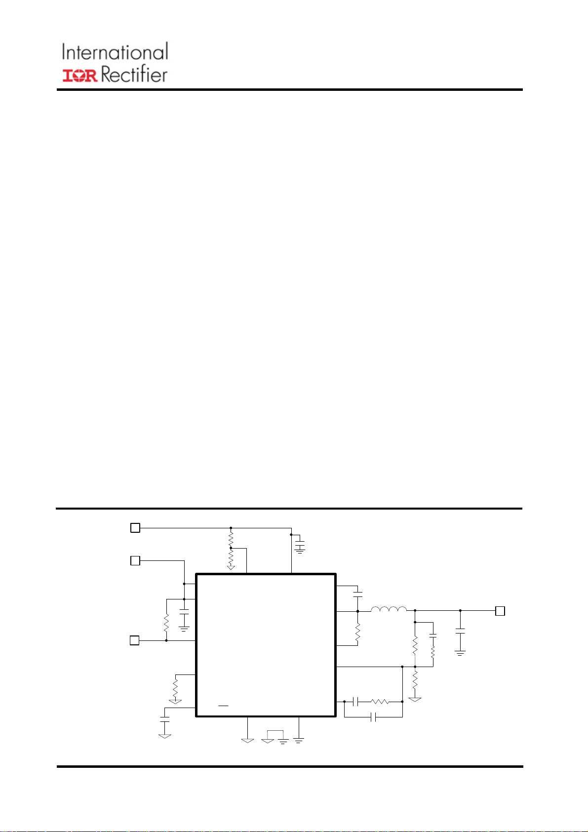
1.5V <Vin<16V
4.5V <Vcc<5.5V
PGood
Seq
Vcc
PGood
Rt
SS/ SD
Enable
Gnd
• Distributed Point of Load Power Architectures
• Netcom Applications
• Computing Peripheral Voltage Regulators
• General DC-DC Converters
Vin
Boot
SW
OCSet
Fb
Comp
PGnd
Vo
Rev 12.0
Fig. 1. Typical application diagram
1
PD-97657
IR3840WMPbF
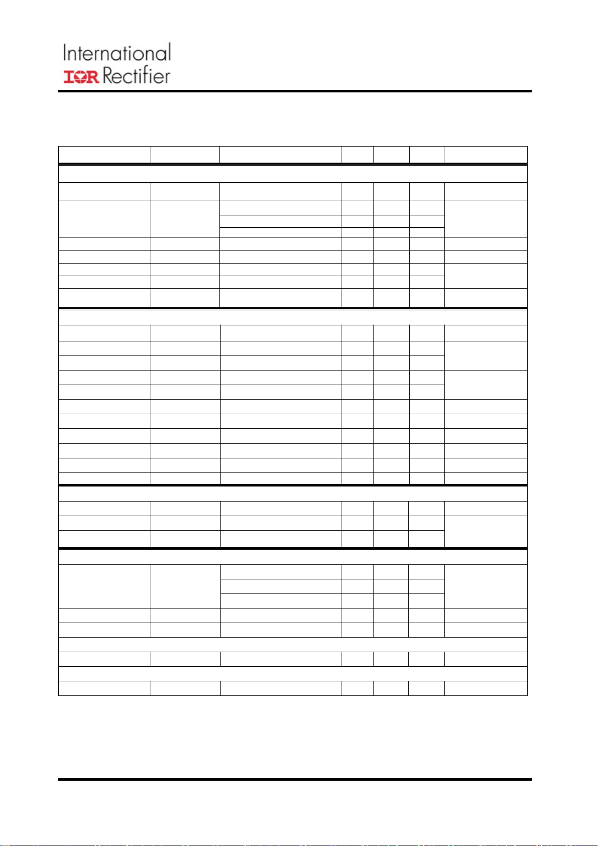
ABSOLUTE MAXIMUM RATINGS
(Voltages referenced to GND unless otherwise specified)
• Vin ……………………………………………………. -0.3V to 25V
• Vcc ……………….….…………….……..……….…… -0.3V to 8V (Note2)
• Boot ……………………………………..……….…. -0.3V to 33V
• SW …………………………………………..……… -0.3V to 25V(DC), -4V to 25V(AC, 100ns)
• Boot to SW ……..…………………………….…..….. -0.3V to Vcc+0.3V (Note1)
• OCSet ………………………………………….……. -0.3V to 30V, 30mA
• Input / output Pins ……………………………….. ... -0.3V to Vcc+0.3V (Note1)
• PGND to GND ……………...………………………….. -0.3V to +0.3V
• Storage Temperature Range ................................... -55°C To 150°C
• Junction Temperature Range ................................... -40°C To 150°C (Note2)
• ESD Classification …………………………… ……… JEDEC Class 1C
• Moisture sensitivity level………………...………………JEDEC Level 2@260 °C (Note5)
Note1: Must not exceed 8V
Note2: Vcc must not exceed 7.5V for Junction Temperature between -10
o
C and -40oC
Stresses beyond those listed under “Absolute Maximum Ratings” may cause permanent damage to the
device. These are stress ratings only and functional operation of the device at these or any other
conditions beyond those indicated in the operational sections of the specifications are not implied.
PACKAGE INFORMATION
SW
5mm x 6mm POWER QFN
V
ORDERING INFORMATION
IN
Boot
Enable
12
13
14
1
23
Seq FB COMP Gnd Rt SS OCSet
15
Gnd
4
11
PGnd
10
=
JA
-
PCBJ
V
9
8
5
7
6
CC
PGood
=
o
W/C35θ
o
W/C2θ
Rev 12.0
PACKAGE
DESIGNATOR
M
PACKAGE
DESCRIPTION
IR3840WMTR1PbF
PIN
COUNT
15
PARTS PER
REEL
400015IR3840WMTRPbFM
750
2
PD-97657
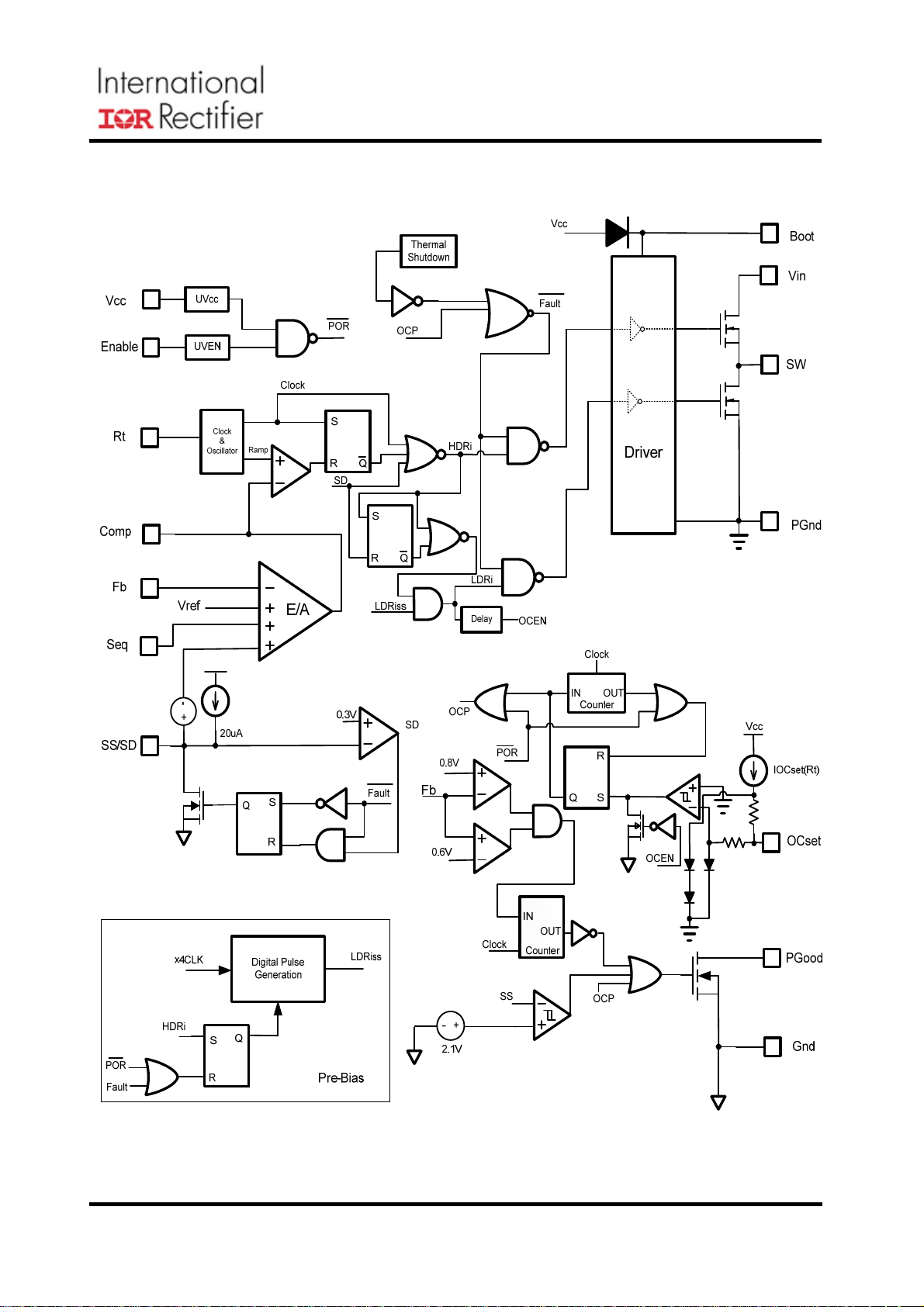
Block Diagram
IR3840WMPbF
Rev 12.0
Fig. 2. Simplified block diagram of the IR3840W
3

PD-97657
Pin Description
Pin Name Description
1 Seq
2 Fb
3 Comp
4 Gnd Signal ground for internal reference and control circuitry.
5 Rt
6 SS/SD¯¯
7 OCSet
Sequence pin. Use two external resistors to set Simultaneous Power up
sequencing. If this pin is not used connect to Vcc.
Inverting input to the error amplifier. This pin is connected directly to the
output of the regulator via resistor divider to set the output voltage and
provide feedback to the error amplifier.
Output of error amplifier. An external resistor and capacitor network is
typically connected from this pin to Fb pin to provide loop
compensation.
Set the switching frequency. Connect an external resistor from this pin
to Gnd to set the switching frequency.
Soft start / shutdown. This pin provides user programmable soft-start
function. Connect an external capacitor from this pin to Gnd to set the
start up time of the output voltage. The converter can be shutdown by
pulling this pin below 0.3V.
Current limit set point. A resistor from this pin to SW pin will set the
current limit threshold.
IR3840WMPbF
8 PGood
9
10 PGnd
11
12
13 Boot
14 Enable
15 Gnd Signal ground for internal reference and control circuitry.
V
CC
SW
V
IN
Power Good status pin. Output is open drain. Connect a pull up resistor
from this pin to Vcc. If unused, it can be left open.
This pin powers the internal IC and the drivers. A minimum of 1uF high
frequency capacitor must be connected from this pin to the power
ground (PGnd).
Power Ground. This pin serves as a separated ground for the MOSFET
drivers and should be connected to the system’s power ground plane.
Switch node. This pin is connected to the output inductor.
Input voltage connection pin.
Supply voltage for high side driver. A 0.1uF capacitor must be
connected from this pin to SW.
Enable pin to turn on and off the device. Use two external resistors to
set the turn on threshold (see Enable section). Connect this pin to Vcc if
it is not used.
Rev 12.0
4
PD-97657
IR3840WMPbF
Recommended Operating Conditions
Symbol Definition Min Max Units
V
mΩ
%
Vin Input Voltage 1.5 16
Vcc Supply Voltage 4.5 5.5
Boot to SW Supply Voltage 4.5 5.5
Vo Output Voltage 0.7 0.9*Vin
Io Output Current 0 12 A
Fs Switching Frequency 225 1650 kHz
Tj Junction Temperature -40 125 oC
Electrical Specifications
Unless otherwise specified, these specification apply over 4.5V< Vcc<5.5V, Vin=12V, 0oC<Tj< 125oC.
Typical values are specified at T
Parameter Symbol Test Condition Min TYP MAX Units
Power Loss
Power Loss P
MOSFET R
Top Switch R
Bottom Switch R
Reference Voltage
Feedback Voltage VFB 0.7 V
ds(on)
= 25oC.
a
Vcc=5V, Vin=12V, Vo=1.8V, Io=12A,
loss
ds(on)_Top
ds(on)_Bot
Fs=600kHz, L=0.6uH, Note4
V
=5V, ID=14A, Tj=250C
Boot -Vsw
Vcc=5V, ID=14A, Tj=250C
0oC<Tj<125oC -1.0 +1.0 Accuracy
o
C<Tj<125oC,
-40
Note3
-2.0 +2.0
2.5 W
8.4 10.6
5.7 6.9
Supply Current
Vcc Supply Current (Standby)
Vcc Supply Current (Dyn) I
I
SS=0V, No Switching, Enable low 500 uA
CC(Standby)
SS=3V, Vcc=5V, Fs=500kHz
CC(Dyn)
Enable high
15 mA
Under Voltage Lockout
Vcc-Start-Threshold VCC_UVLO_Start Vcc Rising Trip Level 3.95 4.15 4.35
Vcc-Stop-Threshold VCC_UVLO_Stop Vcc Falling Trip Level 3.65 3.85 4.05
Enable-Start-Threshold Enable_UVLO_Start Supply ramping up 1.14 1.2 1.36
Enable-Stop-Threshold Enable_UVLO_Stop Supply ramping down 0.9 1.0 1.06
Enable leakage current Ien Enable=3.3V 15 uA
V
Rev 12.0
5
PD-97657
IR3840WMPbF
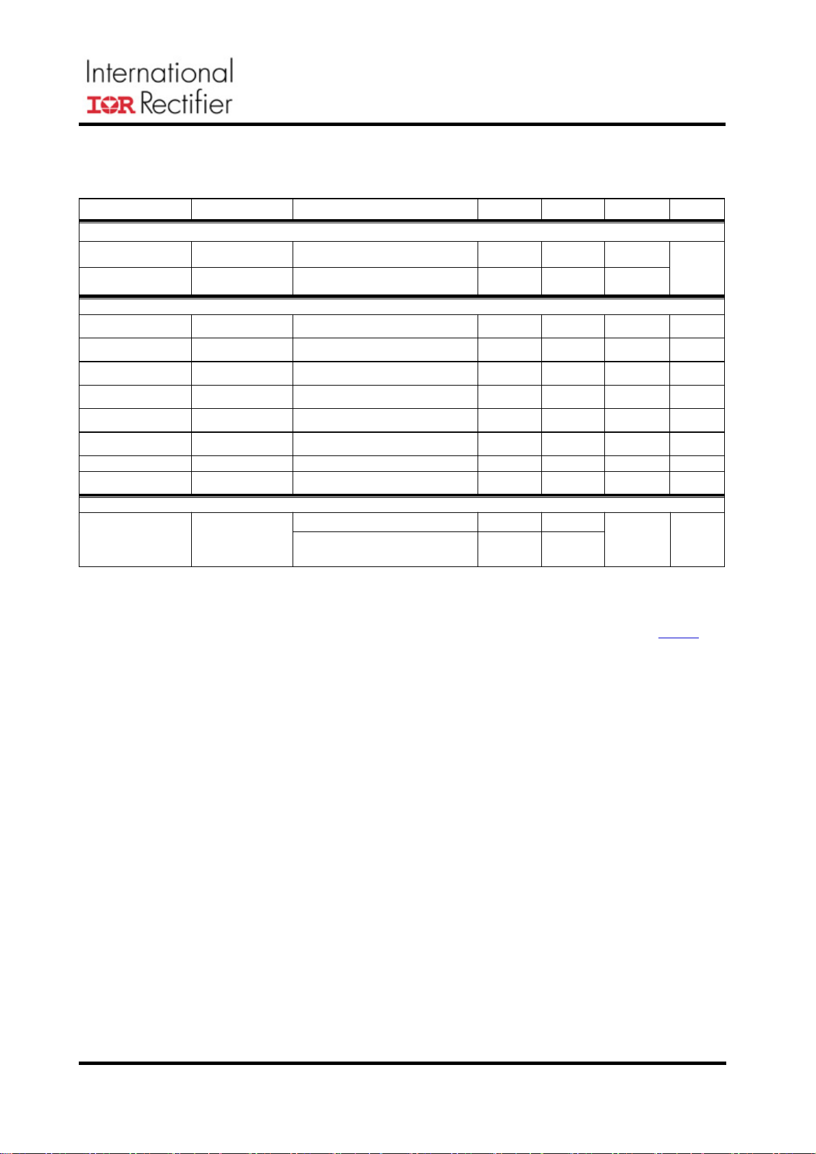
Electrical Specifications (continued)
Unless otherwise specified, these specification apply over 4.5V< Vcc<5.5V, Vin=12V, 0oC<Tj< 125oC.
Typical values are specified at T
Parameter Symbol Test Condition Min TYP MAX Units
Oscillator
Rt Voltage
Frequency F
Ramp Amplitude Vramp
Ramp Offset Ramp (os)
Min Pulse Width Dmin(ctrl)
Fixed Off Time
Max Duty Cycle Dmax Fs=250kHz 92 %
Error Amplifier
Input Offset Voltage Vos Vfb-Vseq,
Input Bias Current IFb(E/A) -1 +1
Input Bias Current IVp(E/A) -1 +1
Sink Current Isink(E/A) 0.40 0.85 1.2
Source Current Isource(E/A) 8 10 13
Slew Rate SR
Gain-Bandwidth Product GBWP
DC Gain Gain
Maximum Voltage Vmax(E/A)
Minimum Voltage Vmin(E/A)
Common Mode Voltage
Soft Start/SD
Soft Start Current ISS Source 14 20 26
Soft Start Clamp Voltage Vss(clamp) 2.7 3.0 3.3
Shutdown Output
Threshold
Over Current Protection
OCSET Current I
OC Comp Offset Voltage V
SS off time SS_Hiccup 4096 Cycles
Bootstrap Diode
Forward Voltage I(Boot)=30mA 180 260 470 mV
Deadband
Deadband time
= 25oC.
a
S
SD 0.3
OCSET
OFFSET
Rt=59K 225 250 275
Rt=28.7K 450 500 550
Rt=9.31K, Note4
Note4
Note4
Note4
Note4
Vseq=0.8V
Note4
Note4
Note4
Vcc=4.5V
Note4
Fs=250kHz 20.8 23.6 26.4
Fs=500kHz 43 48.8 54.6
Fs=1500kHz 136 154 172
Note4
Note4
0.665 0.7 0.735 V
1350 1500 1650
1.8 Vp-p
0.6 V
50
130 200
-10 0 +10 mV
7 12 20
20 30 40 MHz
100 110 120 dB
3.4 3.5 3.75 V
120 220 mV
0 1 V
-10 0 +10 mV
5 10 30 ns
kHz
ns
μA
mA
V/μs
μA
V
μA
Rev 12.0
6
PD-97657
IR3840WMPbF
Electrical Specifications (continued)
Unless otherwise specified, these specification apply over 4.5V< Vcc<5.5V, Vin=12V, 0oC<Tj< 125oC.
Typical values are specified at T
Parameter SYM Test Condition Min TYP MAX Units
Thermal Shutdown
Thermal Shutdown
Hysteresis
Power Good
Power Good upper
Threshold
Upper Threshold
Delay
Power Good lower
Threshold
Lower Threshold
Delay
Delay Comparator
Threshold
Delay Comparator
Hysteresis
PGood Voltage Low PG(voltage) I
Leakage Current I
VPG(upper) Fb Rising 0.770 0.805 0.840 V
VPG(upper)_Dly Fb Rising 256/Fs s
VPG(lower) Fb Falling 0.560 0.595 0.630 V
VPG(lower)_Dly Fb Falling 256/Fs s
PG(Delay) Relative to charge voltage, SS rising 2 2.1 2.3 V
Delay(hys)
leakage
= 25oC.
a
Note4 140
Note4 20
Note4
=-5mA 0.5 V
PGood
0 10
260 300 340 mV
o
μA
C
Switch Node
Isw
SW=0V, Enable=0V SW Bias Current
SW=0V,Enable=high,SS=3V,Vseq=0V,
Note4
6
μA
Note3: Cold temperature performance is guaranteed via correlation using statistical quality control. Not tested in production.
Note4: Guaranteed by Design but not tested in production.
Note5: Upgrade to industrial/MSL2 level applies from date codes 1227 (marking explained on application note AN1132
Products with prior date code of 1227 are qualified with MSL3 for Consumer market.
page 2).
Rev 12.0
7
V
PD-97657
IR3840WMPbF
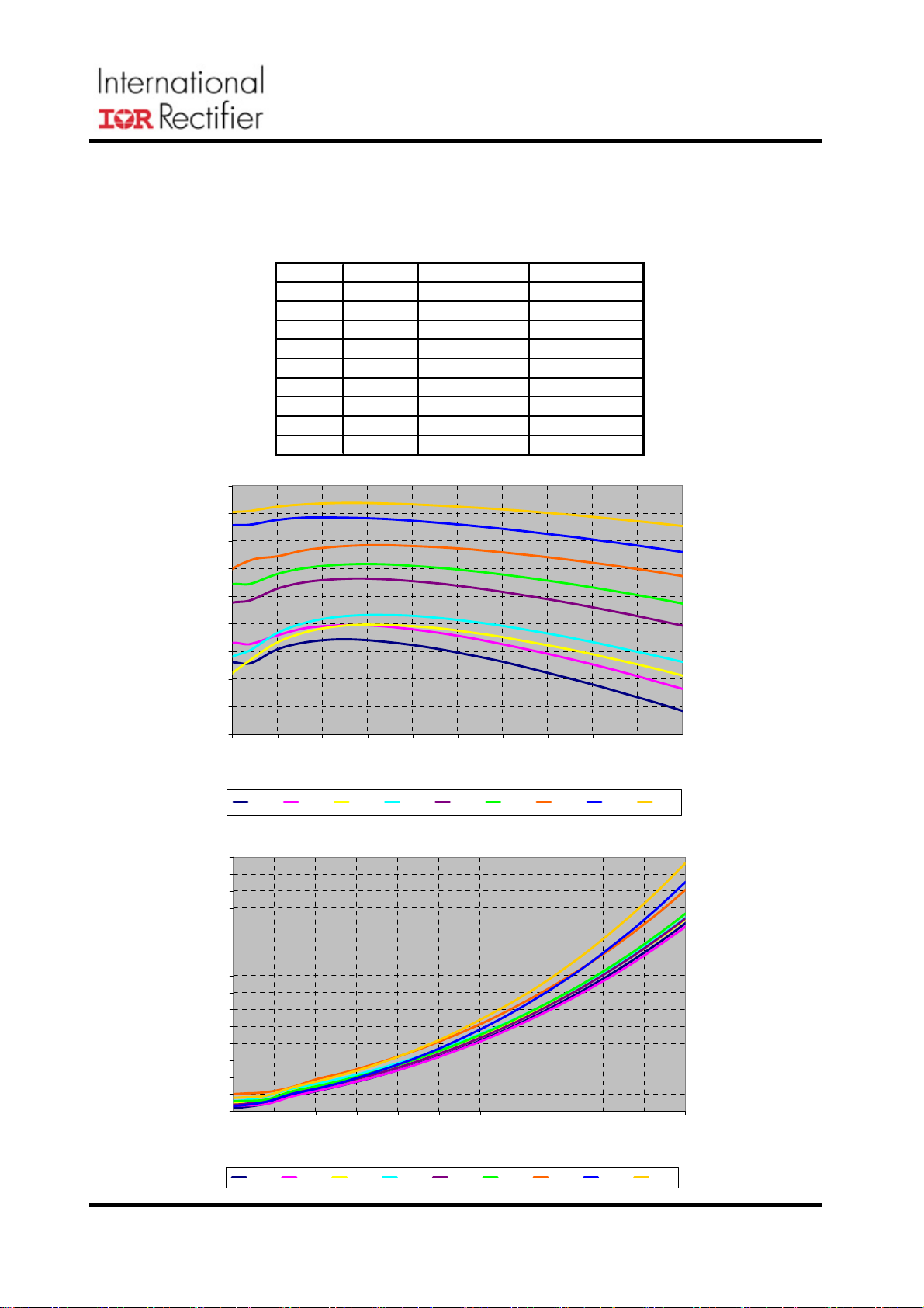
Typical Efficiency and Power Loss Curves
Vin=12V, Vcc=5V, Io=2A-12A, F
=600kHz, Room Temperature, No Air Flow
s
The table below shows the inductors used for each of the output voltages
in the efficiency measurement.
o (V) L (uH) P/N DCR (mOHm)
0.9 0.3 59PR9874N 0.29
1.0 0.3 59PR9874N 0.29
1.1 0.4 59PR9875N 0.29
1.2 0.4 59PR9875N 0.29
1.5 0.5 59PR9876N 0.29
1.8 0.5 59PR9876N 0.29
2.5 0.6 MPL104-0R6 1.5
3.3 1.0 MPL105-1R0 2.3
5.0 1.0 MPL105-1R0 2.3
98
96
94
92
90
88
Efficiency (%)
86
84
82
80
23456789101112
Load Current (A)
0.9V 1.0V 1.1V 1.2V 1.5V 1.8V 2.5V 3.3V 5.0V
3.2
3.0
2.8
2.6
2.4
2.2
2.0
1.8
1.6
1.4
1.2
Power Loss (W)
1.0
0.8
0.6
0.4
0.2
123456789101112
Load Current (A)
0.9V 1.0V 1.1V 1.2V 1.5V 1.8V 2.5V 3.3V 5.0V
Rev 12.0
8
PD-97657
IR3840WMPbF
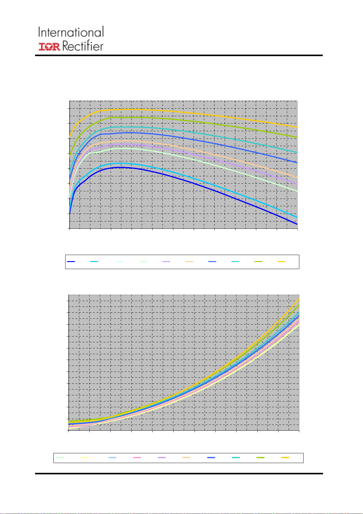
Typical Efficiency and Power Loss Curves
Vin=5V, Vcc=5V, Io=1A-12A, Fs=600kHz, Room Temperature, No Air Flow
For all the output voltages, L=0.3uH (DCR=0.29 mΩ, P/N: 59PR9874N)
97
95
93
91
89
Efficiency (%)
87
85
83
81
1.0 2.0 3.0 4.0 5.0 6.0 7.0 8.0 9.0 10.0 11.0 12.0
Load Current (A)
0.7V 0.75V 0.9V 1.0V 1.1V 1.2V 1.5V 1.8V 2.5V 3.3V
2.3
2.1
1.9
1.7
1.5
1.3
1.1
0.9
Power Loss (W)
0.7
0.5
0.3
0.1
Rev 12.0
123456789101112
Load Current (A)
0.7V 0.75V 0.9V 1.0V 1.1V 1.2V 1.5V 1.8V 2.5V 3.3V
9
PD-97657
IR3840WMPbF
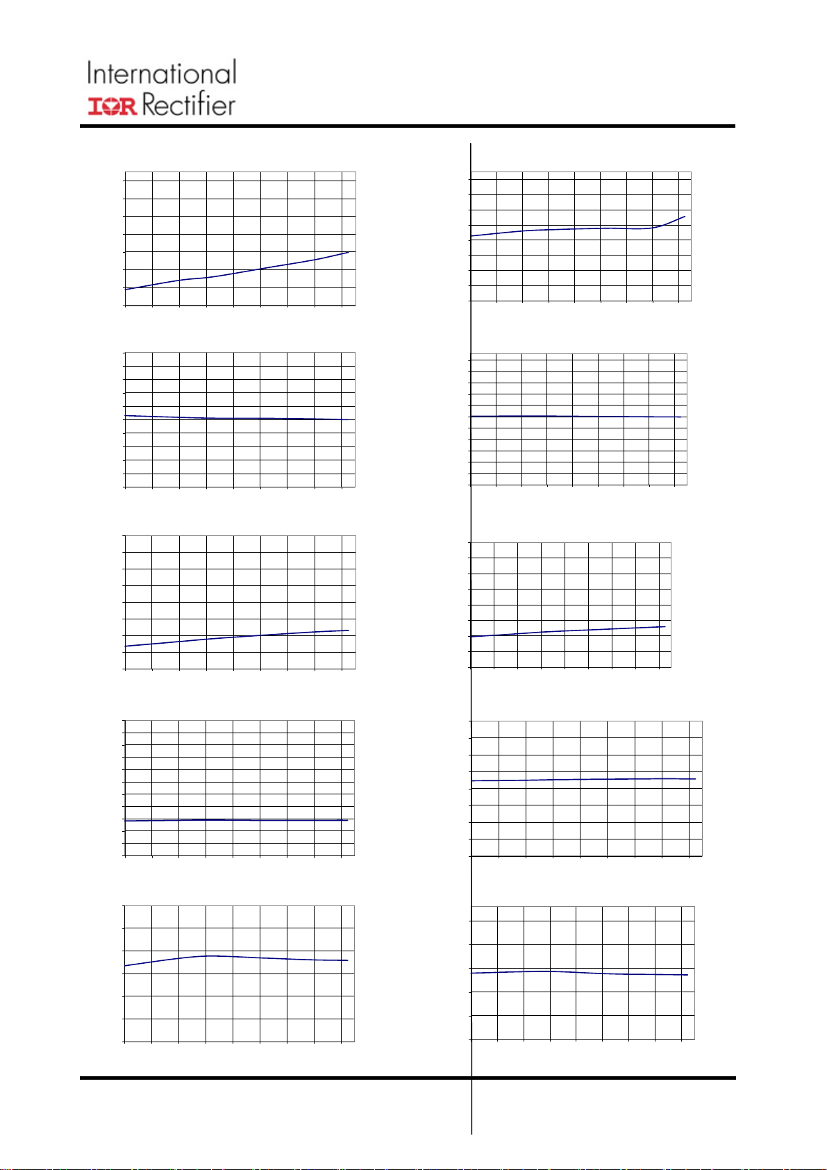
TYPICAL OPERATING CHARACTERISTICS (-40oC - 125oC) Fs=500 kHz
Icc(Standby)
290
270
250
230
[uA]
210
190
170
150
-40 -20 0 20 40 60 80 100 120
550
540
530
520
510
500
[kHz]
490
480
470
460
450
-40 -20 0 20 40 60 80 100 120
4.46
4.41
4.36
4.31
4.26
[V]
4.21
4.16
4.11
4.06
-40-200 20406080100120
Temp[ oC]
FREQUENCY
Temp[
Vcc(UVLO) Start
o
C]
Temp[ oC]
1.36
Enable(UVLO) Start
1.34
1.32
1.30
1.28
1.26
[V]
1.24
1.22
1.20
1.18
1.16
1.14
-40 -20 0 20 40 60 80 100 120
Temp[ oC]
26.0
24.0
22.0
20.0
[uA]
18.0
16.0
14.0
-40-200 20406080100120
ISS
Temp[ oC]
13.5
12.5
11.5
10.5
9.5
[mA]
8.5
7.5
6.5
5.5
-40-200 20406080100120
54.0
53.0
52.0
51.0
50.0
49.0
[uA]
48.0
47.0
46.0
45.0
44.0
43.0
-40-20 0 20406080100120
4.16
4.11
4.06
4.01
3.96
[V]
3.91
3.86
3.81
3.76
-40-20 0 20406080100120
1.06
1.04
1.02
1.00
0.98
[V]
0.96
0.94
0.92
0.90
-40 -20 0 20 40 60 80 100 120
711
706
701
[mV]
696
691
686
-40-20 0 20406080100120
Icc(Dyn)
Temp[ oC]
IOCSET(500kHz)
Temp[ oC]
Vcc(UVLO) Stop
Temp[ oC]
Enable(UVLO) Stop
Temp[
Vfb
Temp[ oC]
ο
C]
Rev 12.0
10
PD-97657
Rdson of MOSFETs Over Temperature at Vcc=5V
12
11
10
]
Ω
9
8
7
Resistance [m
6
5
4
-40 -20 0 20 40 60 80 100 120 140
Temperature [°C]
IR3840WMPbF
Sync-FET Ctrl-FET
Thermal De-rating Curves
Test Conditions: Vin=12V, Vout=1.8V, Vcc=5V, Fs=600kHz, 0- 400LFM
L=0.6uH (MPL104-0R6IR)
12.5
12
11.5
11
10.5
10
Maximum Load Curent (A)
9.5
Rev 12.0
9
25 30 35 40 45 50 55 60 65 70 75 80 85
Ambient Temperature [°C]
0 LFM 100 LFM 200 LFM 300 LFM 400 LFM
11

PD-97657
Circuit Description
THEORY OF OPERATION
Introduction
The IR3840W uses a PWM voltage mode control
scheme with external compensation to provide
good noise immunity and maximum flexibility in
selecting inductor values and capacitor types.
The switching frequency is programmable from
250kHz to 1.5MHz and provides the capability of
optimizing the design in terms of size and
performance.
IR3840W provides precisely regulated output
voltage programmed via two external resistors
from 0.7V to 0.9*Vin.
The IR3840W operates with an external bias
supply from 4.5V to 5.5V, allowing an extended
operating input voltage range from 1.5V to 16V.
IR3840WMPbF
If the input to the Enable pin is derived from the
bus voltage by a suitably programmed resistive
divider, it can be ensured that the IR3840W does
not turn on until the bus voltage reaches the
desired level. Only after the bus voltage reaches
or exceeds this level will the voltage at Enable
pin exceed its threshold, thus enabling the
IR3840W. Therefore, in addition to being a logic
input pin to enable the IR3840W, the Enable
feature, with its precise threshold, also allows the
user to implement an Under-Voltage Lockout for
the bus voltage V
for high output voltage applications, where we
might want the IR3840W to be disabled at least
until V
exceeds the desired output voltage level.
in
. This is desirable particularly
in
The device utilizes the on-resistance of the low
side MOSFET as current sense element, this
method enhances the converter’s efficiency and
reduces cost by eliminating the need for external
current sense resistor
IR3840W includes two low R
using IR’s HEXFET technology. These are
specifically designed for high efficiency
applications.
Under-Voltage Lockout and POR
The under-voltage lockout circuit monitors the
input supply Vcc and the Enable input. It assures
that the MOSFET driver outputs remain in the off
state whenever either of these two signals drop
below the set thresholds. Normal operation
resumes once Vcc and Enable rise above their
thresholds.
The POR (Power On Ready) signal is generated
when all these signals reach the valid logic level
(see system block diagram). When the POR is
asserted the soft start sequence starts (see soft
start section).
.
MOSFETs
ds(on)
Fig. 3a. Normal Start up, Device turns on
when the Bus voltage reaches 10.2V
Figure 3b. shows the recommended start-up
sequence for the non-sequenced operation of
IR3840W, when Enable is used as a logic input.
Enable
The Enable features another level of flexibility for
start up. The Enable has precise threshold which
is internally monitored by Under-Voltage Lockout
(UVLO) circuit. Therefore, the IR3840W will turn
on only when the voltage at the Enable pin
exceeds this threshold, typically, 1.2V.
Rev 12.0
Fig. 3b. Recommended startup sequence,
Non-Sequenced operation
12

(
PD-97657
Figure 3c. shows the recommended startup
sequence for sequenced operation of IR3840W
with Enable used as logic input.
Fig. 3c. Recommended startup sequence,
Sequenced operation
Pre-Bias Startup
IR3840W is able to start up into pre-charged
output, which prevents oscillation and
disturbances of the output voltage.
The output starts in asynchronous fashion and
keeps the synchronous MOSFET off until the first
gate signal for control MOSFET is generated.
Figure 4 shows a typical Pre-Bias condition at
start up.
The synchronous MOSFET always starts with a
narrow pulse width and gradually increases its
duty cycle with a step of 25%, 50%, 75% and
100% until it reaches the steady state value. The
number of these startup pulses for the
synchronous MOSFET is internally programmed.
Figure 5 shows a series of 32, 16, 8 startup
pulses.
IR3840WMPbF
Fig. 5. Pre-Bias startup pulses
Soft-Start
The IR3840W has a programmable soft-start to
control the output voltage rise and to limit the
current surge at the start-up. To ensure correct
start-up, the soft-start sequence initiates when
the Enable and Vcc rise above their UVLO
thresholds and generate the Power On Ready
(POR) signal. The internal current source
(typically 20uA) charges the external capacitor
C
linearly from 0V to 3V. Figure 6 shows the
ss
waveforms during the soft start.
The start up time can be estimated by:
)
C
*0.7-1.4
T =
start
During the soft start the OCP is enabled to
protect the device for any short circuit and over
current condition.
SS
μ
A20
(1) --------------------
Fig. 6. Theoretical operation waveforms
during soft-start
Fig. 4. Pre-Bias startup
Rev 12.0
13

∗
=
PD-97657
Operating Frequency
The switching frequency can be programmed
between 250kHz – 1500kHz by connecting an
external resistor from R
tabulates the oscillator frequency versus R
Table 1. Switching Frequency and I
External Resistor (R
(kΩ)
(kΩ)
t
t
pin to Gnd. Table 1
t
)
t
I
I
ocset
ocset
29.430047.5
29.430047.5
39.240035.7
39.240035.7
48.750028.7
48.750028.7
59.0760023.7
59.0760023.7
68.270020.5
68.270020.5
78.680017.8
78.680017.8
88.690015.8
88.690015.8
97.9100014.3
97.9100014.3
110.2110012.7
110.2110012.7
121.7120011.5
121.7120011.5
130.8130010.7
130.8130010.7
143.414009.76
143.414009.76
150.315009.31
150.315009.31
OCSet
(μA)Fs (kHz)R
(μA)Fs (kHz)R
.
t
vs.
IR3840WMPbF
1400
I
OCSet
Table 1. shows I
frequencies. The internal current source
develops a voltage across R
side MOSFET is turned on, the inductor current
flows through the Q2 and results in a voltage at
OCSet which is given by:
Fig. 7. Connection of over current sensing resistor
)μA(Ω=
)(k
R
t
at different switching
OCSet
. When the low
OCSet
OCSetOCSetOCSet
RRIV
∗−
L
)
(onDS
.(3).......... ) () (
)2.....(..............................
I
Shutdown
The IR3840W can be shutdown by pulling the
Enable pin below its 1 V threshold. This will tristate both, the high side driver as well as the low
side driver. Alternatively, the output can be
shutdown by pulling the soft-start pin below 0.3V.
Normal operation is resumed by cycling the
voltage at the Soft Start pin.
Over-Current Protection
The over current protection is performed by
sensing current through the R
DS(on)
of low side
MOSFET. This method enhances the converter’s
efficiency and reduces cost by eliminating a
current sense resistor. As shown in figure 7, an
external resistor (R
) is connected between
OCSet
OCSet pin and the switch node (SW) which sets
the current limit set point.
An internal current source sources current (I
OCSet
) out of the OCSet pin. This current is a function
of the switching frequency and hence, of R
.
t
An over current is detected if the OCSet pin goes
below ground. Hence, at the current limit
threshold, V
setting I
Limit,ROCSet
R
OCSet
=
=0. Then, for a current limit
OCset
is calculated as follows:
*
IR
)(
LimitonDS
I
OCSet
(4) ........................
An overcurrent detection trips the OCP
comparator, latches OCP signal and cycles the
soft start function in hiccup mode.
The hiccup is performed by shorting the soft-start
capacitor to ground and counting the number of
switching cycles. The Soft Start pin is held low
until 4096 cycles have been completed. The
OCP signal resets and the converter recovers.
After every soft start cycle, the converter stays in
this mode until the overload or short circuit is
removed.
The OCP circuit starts sampling current typically
160 ns after the low gate drive rises to about 3V.
This delay functions to filter out switching noise.
Rev 12.0
14

PD-97657
Thermal Shutdown
Temperature sensing is provided inside
IR3840W. The trip threshold is typically set to
o
140
C. When trip threshold is exceeded, thermal
shutdown turns off both MOSFETs and
discharges the soft start capacitor.
Automatic restart is initiated when the sensed
temperature drops within the operating range.
There is a 20
shutdown threshold.
Output Voltage Sequencing
The IR3840W can accommodate user
programmable sequencing options using Seq,
Enable and Power Good pins.
o
C hysteresis in the thermal
Vo1
Vo2
1.5V <Vin<16V
4.5V <Vcc<5.5V
PGood
1.5V <Vin<16V
4.5V <Vcc<5.5V
Vo(master)
PGood
RE
RF
Vcc
PGood
Seq
Rt
SS/ SD
IR3840WMPbF
Enable
Vcc
PGood
Seq
Rt
SS/ SD
Gnd
Enable
Gnd
Vin
PGnd
Vin
PGnd
Boot
SW
OCSet
Fb
Comp
Boot
SW
OCSet
Fb
Comp
Vo(master)
RA
RB
Vo(slave)
RC
RD
Simultaneous Powerup
Fig. 8a. Simultaneous Power-up of the slave
with respect to the master.
Through these pins, voltage sequencing such as
simultaneous and sequential can be
implemented. Figure 8. shows simultaneous
sequencing configurations. In simultaneous
power-up, the voltage at the Seq pin of the slave
reaches 0.7V before the Fb pin of the master. For
R
E/RF=RC/RD
, therefore, the output voltage of
the slave follows that of the master until the
voltage at the Seq pin of the slave reaches 0.7 V.
After the voltage at the Seq pin of the slave
exceeds 0.85V, the internal 0.7V reference of
the slave dictates its output voltage.
Fig. 8b. Application Circuit for Simultaneous
Sequencing
Power Good Output
The IC continually monitors the output voltage via
Feedback (Fb pin). The feedback voltage forms
an input to a window comparator whose upper
and lower thresholds are 0.805V and 0.595V
respectively. Hence, the Power Good signal is
flagged when the Fb pin voltage is within the
PGood window, i. e., between 0.595V to 0.805V,
as shown in Fig .9 The PGood pin is open drain
and it needs to be externally pulled high. High
state indicates that output is in regulation. Fig. 9a
shows the PGood timing diagram for nontracking operation. In this case, during startup,
PGood goes high after the SS voltage reaches
2.1V if the Fb voltage is within the PGood
comparator window. Fig. 9a. and Fig 9.b. also
show a 256 cycle delay between the Fb voltage
entering within the thresholds defined by the
PGood window and PGood going high.
Rev 12.0
15

PD-97657
IR3840WMPbF
TIMING DIAGRAM OF PGOOD FUNCTION
Fig.9a IR3840W Non-Tracking Operation (Seq=Vcc)
Rev 12.0
Fig.9b IR3840W Tracking Operation
16

PD-97657
Minimum on time Considerations
The minimum ON time is the shortest amount of
time for which the Control FET may be reliably
turned on, and this depends on the internal
timing delays. For the IR3840W, the typical
minimum on-time is specified as 50 ns.
Any design or application using the IR3840W
must ensure operation with a pulse width that is
higher than this minimum on-time and preferably
higher than 100 ns. This is necessary for the
circuit to operate without jitter and pulseskipping, which can cause high inductor current
ripple and high output voltage ripple.
D
t
on
In any application that uses the IR3840W, the
following condition must be satisfied:
(min)
t
(min)
on
The minimum output voltage is limited by the
reference voltage and hence V
Therefore, for V
=
F
=
in
tt
≤
≤∴
FV
sin
out(min)
s
V
out
V
×
onon
V
V
≤×∴
t
on
= 0.7 V,
F
out
s
×
out
(min)
FV
sin
out(min)
= 0.7 V.
IR3840WMPbF
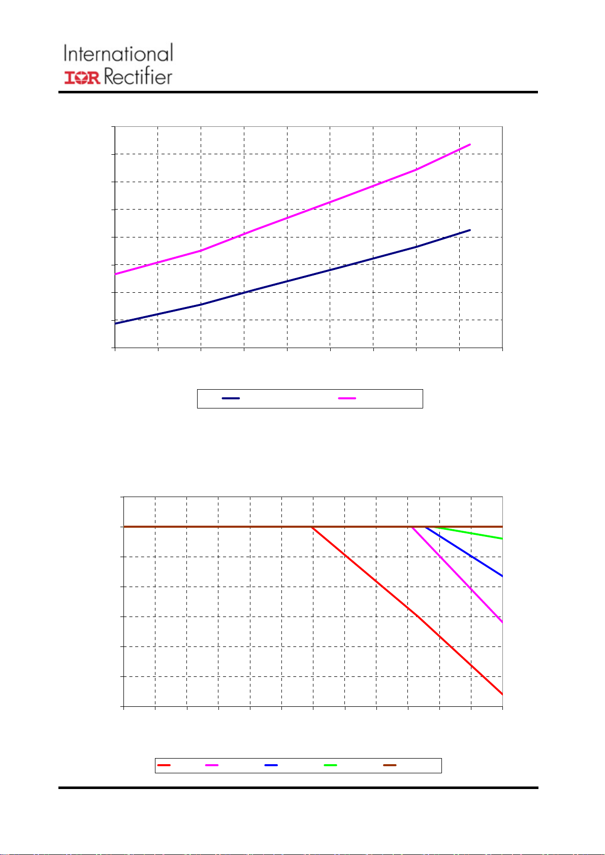
Maximum Duty Ratio Considerations
A fixed off-time of 200 ns maximum is specified
for the IR3840W. This provides an upper limit on
the operating duty ratio at any given switching
frequency. It is clear, that higher the switching
frequency, the lower is the maximum duty ratio at
which the IR3840W can operate. To allow a
margin of 50ns, the maximum operating duty
ratio in any application using the IR3840W
should still accommodate about 250 ns off-time.
Fig 10. shows a plot of the maximum duty ratio
v/s the switching frequency, with 250 ns off-time.
Max Duty Cycle
95
90
85
80
75
70
65
60
Max Duty Cycle (%)
55
250 450 650 850 1050 1250 1450 1650
Switching Frequency (kH z)
Fig. 10. Maximum duty cycle v/s switching
frequency.
V
V
≤×∴
F
in
s
V
F
in
s
(min)
out
t
on
(min)
V0.7
6
V/s
ns 100
107 ×=≤×∴
Therefore, at the maximum recommended input
voltage 16V and minimum output voltage, the
converter should be designed at a switching
frequency that does not exceed 440 kHz.
Conversely, for operation at the maximum
recommended operating frequency 1.65 MHz
and minimum output voltage, any voltage above
4.2 V may not be stepped down without pulseskipping.
Rev 12.0
17

−
≅
=
PD-97657
Application Information
Design Example:
The following example is a typical application for
IR3840W. The application circuit is shown on
page 23.
V
V
I
ΔV
F
in
V1.8=
o
A12 =
o
54mV
≤
o
s
kHz 600=
max)13.2V ( V 12=
Enabling the IR3840W
As explained earlier, the precise threshold of
the Enable lends itself well to implementation of
a UVLO for the Bus Voltage.
V
in
IR3840W
R
1
Enable
R
2
For a typical Enable threshold of V
R
V
For a V
(min)
=
in (min)
RR
2
RR
+
21
V
min
EN
−
12
==
ENin
VV
EN)in(
=10.2V, R1=49.9K and R2=7.5K is a
good choice.
Programming the frequency
For Fs= 600 kHz, select Rt= 23.7 kΩ, using
Table. 1.
Output Voltage Programming
Output voltage is programmed by reference
voltage and external voltage divider. The Fb pin
is the inverting input of the error amplifier, which
is internally referenced to 0.7V. The divider is
ratioed to provide 0.7V at the Fb pin when the
output is at its desired value. The output voltage
is defined by using the following equation:
⎛
⎜
VV
refo
⎜
⎝
⎞
R
8
⎟
+∗=
1
⎟
R
9
⎠
EN
= 1.2 V
(6) ..........
V
(5) .......... 1.2*
.....(7)..............................
IR3840WMPbF
When an external resistor divider is connected to
the output as shown in figure 11.
Equation (5) can be rewritten as:
⎛
⎜
∗=
RR
89
⎜
⎝
For the calculated values of R8 and R9 see
feedback compensation section.
IR3840W
IR3624
Fig. 11. Typical application of the IR3840W for
programming the output voltage
Soft-Start Programming
The soft-start timing can be programmed by
selecting the soft-start capacitance value. From
(1), for a desired start-up time of the converter,
the soft start capacitor can be calculated by
using:
Where T
is the desired start-up time (ms).
start
For a start-up time of 3.5ms, the soft-start
capacitor will be 0.099μF. Choose a 0.1μF
ceramic capacitor.
Bootstrap Capacitor Selection
To drive the Control FET, it is necessary to
supply a gate voltage at least 4V greater than
the voltage at the SW pin, which is connected
the source of the Control FET . This is achieved
by using a bootstrap configuration, which
comprises the internal bootstrap diode and an
external bootstrap capacitor (C6), as shown in
Fig. 12. The operation of the circuit is as follows:
When the lower MOSFET is turned on, the
capacitor node connected to SW is pulled down
to ground. The capacitor charges towards V
through the internal bootstrap diode, which has a
forward voltage drop V
the bootstrap capacitor C6 is approximately
given as
When the upper MOSFET turns on in the next
cycle, the capacitor node connected to SW rises
to the bus voltage V
C6 is appropriately chosen,
⎞
V
ref
⎟
⎟
−
VV
refo
⎠
V
OUT
R
8
(8) ..................................
Fb
R
9
TC
startSS
. The voltage Vcacross
D
Dccc
. However, if the value of
in
(9) .......... 0.02857 ) ms ( )μF( ×
cc
VVV
(10) ..........................
Rev 12.0
18

Δ
e
PD-97657
the voltage V
unchanged and the voltage at the Boot pin
becomes
Fig. 12. Bootstrap circuit to generate
A bootstrap capacitor of value 0.1uF is suitable
for most applications.
Input Capacitor Selection
The ripple current generated during the on time of
the upper MOSFET should be provided by the
input capacitor. The RMS value of this ripple is
expressed by:
V
D =
V
Where:
D is the Duty Cycle
is the RMS value of the input capacitor
I
RMS
current.
Io is the output current.
For I
=12A and D = 0.15, the I
o
Ceramic capacitors are recommended due to
their peak current capabilities. They also feature
low ESR and ESL at higher frequency which
enables better efficiency. For this application, it is
advisable to have 4x10uF 16V ceramic capacitors
ECJ-3YX1C106K from Panasonic. In addition to
these, although not mandatory, a 1X330uF, 25V
SMD capacitor EEV-FK1E331P may also be
used as a bulk capacitor and is recommended if
the input power supply is not located close to the
converter.
across C6 remains approximately
c
VVVV −+≅
DccinBoot
Vc voltage
oRMS
o
in
−∗∗= 1
RMS
....(12)....................)( DDII
(13) ................................
= 4.28A.
IR3840WMPbF
Inductor Selection
The inductor is selected based on output power,
operating frequency and efficiency requirements.
A low inductor value causes large ripple current,
(11) ........................................
resulting in the smaller size, faster response to a
load transient but poor efficiency and high output
noise. Generally, the selection of the inductor
value can be reduced to the desired maximum
ripple current in the inductor . The optimum
point is usually found between 20% and 50%
ripple of the output current.
For the buck converter, the inductor value for the
desired operating ripple current can be
determined using the following relation:
i
oin
()
t
Δ
VVL
∗−=
oin
Δ
LVV
∗=−
Dt
;
∗=Δ
F
V
o
FiV
Δ∗
*
sin
Where:
=
V
in
=
V
o
=
Δi
=
F
s
=
Δt
=
D
If Δi ≈ 35%(I
VoltageOutput
time on Turn
cycleDuty
), then the output inductor is
o
input Maximum
current ripple Inductor
frequency Switching
calculated to be 0.607μH. Select L=0.6 μH.
The MPL104-0R6 from Delta provides a compact,
low profile inductor suitable for this application.
)( i
1
s
voltag
(14) ...............................
.
Rev 12.0
19

Δ
PD-97657
Output Capacitor Selection
The voltage ripple and transient requirements
determine the output capacitors type and values.
The criteria is normally based on the value of the
Effective Series Resistance (ESR). However the
actual capacitance value and the Equivalent Series
Inductance (ESL) are other contributing
components. These components can be described
as
+Δ+Δ=Δ
VVVV
)()()(
CoESLoESRoo
Δ=Δ
*
)(
⎛
⎜
V
V
o
=Δ
)(
ESLo
⎜
⎝
=Δ
V
)(
Co
=Δ
ESRIV
LESRo
−
VV
⎞
oin
⎟
*
ESL
⎟
L
⎠
Δ
I
L
FC
**
8
so
ripple voltage Output
IR3840WMPbF
The output LC filter introduces a double pole,
–40dB/decade gain slope above its corner
resonant frequency, and a total phase lag of 180
(see figure 13). The resonant frequency of the LC
filter is expressed as follows:
=
LC
Figure 13 shows gain and phase of the LC filter.
Since we already have 180
output filter alone, the system runs the risk of
being unstable.
Gain
(15) .........................
0 dB
1
π
2
-40dB/decade
CLF∗∗
oo
o
phase shift from the
Phase
0
0
o
(16) ................................
=Δ
I
L
current ripple Inductor
Since the output capacitor has a major role in the
overall performance of the converter and
determines the result of transient response,
selection of the capacitor is critical. The
IR3840W can perform well with all types of
capacitors.
As a rule, the capacitor must have low enough
ESR to meet output ripple and load transient
requirements.
The goal for this design is to meet the voltage
ripple requirement in the smallest possible
capacitor size. Therefore it is advisable to select
ceramic capacitors due to their low ESR and ESL
and small size. Six of the Panasonic ECJ2FB0J226ML (22uF, 6.3V, 3mOhm) capacitors is
a good choice.
Feedback Compensation
The IR3840W is a voltage mode controller. The
control loop is a single voltage feedback path
including error amplifier and error comparator. To
achieve fast transient response and accurate
output regulation, a compensation circuit is
necessary. The goal of the compensation
network is to provide a closed-loop transfer
function with the highest 0 dB crossing frequency
o
and adequate phase margin (greater than 45
).
0
F
LC
Frequency
-180
F
LC
Frequency
Fig. 13. Gain and Phase of LC filter
The IR3840W uses a voltage-type error amplifier
with high-gain (110dB) and wide-bandwidth. The
output of the amplifier is available for DC gain
control and AC phase compensation.
The error amplifier can be compensated either in
type II or type III compensation.
Local feedback with Type II compensation is
shown in Fig. 14.
This method requires that the output capacitor
should have enough ESR to satisfy stability
requirements. In general the output capacitor’s
ESR generates a zero typically at 5kHz to 50kHz
which is essential for an acceptable phase
margin.
The ESR zero of the output capacitor is
expressed as follows:
F
ESR
=
∗
2
1
*ESR*C
π
o
(17) ...........................
Rev 12.0
20

=
PD-97657
Fig. 14. Type II compensation network
and its asymptotic gain plot
IR3840WMPbF
Where:
= Maximum Input Voltage
V
in
= Oscillator Ramp Voltage
V
osc
= Crossover Frequency
F
o
= Zero Frequency of the Output Capacitor
F
ESR
= Resonant Frequency of the Output Filter
F
LC
= Feedback Resistor
R
8
To cancel one of the LC filter poles, place the
zero before the LC filter resonant frequency pole:
FF
%
LCz
F
75075=
z
Use equations (20), (21) and (22) to calculate
C4.
One more capacitor is sometimes added in
parallel with C4 and R3. This introduces one
more pole which is mainly used to suppress the
switching noise.
The additional pole is given by:
1
*.
2
CL
π
*
oo
(22) .....................................
The transfer function (Ve/Vo) is given by:
1
V
e
V
o
Z
f
sH
Z
IN
CsR
+
−=−==
43
CsR
48
(18) ..... )(
The (s) indicates that the transfer function varies
as a function of frequency. This configuration
introduces a gain and zero, expressed by:
R
3
()
sH
=
R
8
F
z
1
=
2
π
CR
**
43
(19) ............................. .........
(20) ............................
First select the desired zero-crossover frequency
):
(F
o
≤>
()
o
FFF *1/10~1/5 F and
sESRo
Use the following equation to calculate R3:
***
RFFV
ESRoosc
R =
3
8
2
*
FV
LCin
(21) ...........................
F+=
P
2
π
1
*
CC
POLE
4
**
R
3
CC
POLE
4
...(23)..............................
The pole sets to one half of the switching
frequency which results in the capacitor C
C
POLE
=
1
1
−
*F*R
π
s
3
C
4
1
≅
*F*R
π
s
3
POLE
:
(24)......................
For a general solution for unconditional stability
for any type of output capacitors, and a wide
range of ESR values, we should implement local
feedback with a type III compensation network.
The typically used compensation network for
voltage-mode controller is shown in figure 15.
Again, the transfer function is given by:
By replacing Z
V
e
V
o
and Zfaccording to figure 15,
in
Z
sH
f
−== )(
Z
IN
the transfer function can be expressed as:
[]
−
=
)(
sH
)(
⎡
++
)(
sRCCsR
⎢
⎢
⎣
()
11
⎛
⎜
3348
⎜
⎝
+++
RRsCCsR
108743
⎤
⎞
*
CC
34
⎟
11
+
⎥
⎟
+
CC
⎥
34
⎠
⎦
CsR
710
(25) ....
)(
Rev 12.0
21

(
PD-97657
OUT
C
10
R
Gain(dB)
V
3
C
7
8
R
Fb
9
R
REF
V
3
R
E/A
C
IN
Z
H(s) dB
1
Z
F
2
Z
F
2
P
F
P
F
Fig.15. Type III Compensation network and
its asymptotic gain plot
4
Comp
Frequency
3
IR3840WMPbF
Compensator
Compensator
Type
Type
f
Z
Type III
Ve
Type III
F
F
vs F
vs F
ESR
ESR
F
F
LC<FES R<Fo<Fs
LC<FES R<Fo<Fs
F
F
LC<Fo<FESR
LC<Fo<FESR
The higher the crossover frequency, the
potentially faster the load transient response.
However, the crossover frequency should be low
enough to allow attenuation of switching noise.
Typically, the control loop bandwidth or crossover
frequency is selected such that
)
F F *1/10~1/5≤
so
The DC gain should be large enough to provide
high DC-regulation accuracy. The phase margin
should be greater than 45
o
for overall stability.
o
o
Output
Output
Capacitor
Capacitor
Electrolytic
Electrolytic
/2Type II
/2Type II
Tantalum
Tantalum
Tantalum
Tantalum
Ceramic
Ceramic
The compensation network has three poles and
two zeros and they are expressed as follows:
0
F
=
P
1
F
=
P
2
=
F
P
3
F
=
Z
1
F
=
Z
2
1
2
π
2
π
CR
**
710
1
⎛
⎜
R
*
3
⎜
⎝
≅
⎞
CC
*
34
⎟
⎟
CC
+
34
⎠
1
2
π
CR
**
1
2
π
2
CR
**
43
1
≅
+
1
2
ππ
**)(**
......(26)............................................................
) .......(27........................................
(28) ...............
33
.....(29)........................................
RCRRC
871087
(30)..........
Cross over frequency is expressed as:
V
=
o
in
CRF
73
1
***
**
CLV
π
2
ooosc
(31) ................................
Based on the frequency of the zero generated by
the output capacitor and its ESR, relative to
crossover frequency, the compensation type can
be different. The table below shows the
compensation types for relative locations of the
crossover frequency.
For this design we have:
V
=12V
in
V
=1.8V
o
V
=1.8V
osc
V
=0.7V
ref
L
=0.6uH
o
C
=6x22uF, ESR=3mOhm each
o
It must be noted here that the value of the
capacitance used in the compensator design
must be the small signal value. For instance, the
small signal capacitance of the 22uF capacitor
used in this design is 12uF at 1.8 V DC bias and
600 kHz frequency. It is this value that must be
used for all computations related to the
compensation. The small signal value may be
obtained from the manufacturer’s datasheets,
design tools or SPICE models. Alternatively, they
may also be inferred from measuring the power
stage transfer function of the converter and
measuring the double pole frequency F
LC
and
using equation (16) to compute the small signal
C
.
o
These result to:
F
=24.2 kHz
LC
F
=4.4 MHz
ESR
F
/2=300 kHz
s
Select crossover frequency F
Since FLC<Fo<Fs/2<F
ESR
=100 kHz
o
, TypeIII is selected to
place the pole and zeros.
Rev 12.0
22

PD-97657
Detailed calculation of compensation TypeIII
o
=Θ
70 Margin Phase Desired
Θ−
sin
1
=
FF
oZ
2
1
1
=
FF
oP
2
1
3
R
3
FF
=
7
π
2
R
3
=
Θ+
sin
Θ+
sin
=
Θ−
sin
50
FF
ZZ
==
sP
kHz 17.63
kHz 567.1
==
21
and kHz 8.82 *. :Select
kHz 300*0.5
nF 2.2C :Select
: and , Calculate
CCR
433
*
VCLF
***
oscooo
R
*
VC
in
7
k 1.87 :Select
Ω=
3
kΩ 1.85;
==
IR3840WMPbF
Programming the Current-Limit
The Current-Limit threshold can be set by
connecting a resistor (R
to the OCSet pin. The resistor can be calculated
by using equation (4). This resistor R
be placed close to the IC.
The R
DS(on)
has a positive temperature
coefficient and it should be considered for the
worst case operation.
∗
R
==
==≅
*
==
sOCSet
OCSet
II
)on(DS
==
)(
criticalLSET
75
*
)LIM(oSET
Setting the Power Good Threshold
A window comparator internally sets a lower
Power Good threshold at 0.6V and an upper
Power Good threshold at 0.8V. When the voltage
at the FB pin is within the window set by these
thresholds, PGood is asserted.
) from the SW pin
OCSET
IR
OCSetOCSet
)(
onDS
mΩ 7.1251.25mΩ .R
A 181.5A 12II
kHz) 600F (at μA 59.07I
kΩ 2.15R Select kΩ 2.17R
==
7
OCSET
) current output nominal over (50%
must
(32) .......................
C
4
1
**2
π
RF
Z
1
3
CC
nF 10 :Select nF, 9.65 ;
===
44
The PGood is an open drain output. Hence, it is
necessary to use a pull up resistor R
PG
from
PGood pin to Vcc. The value of the pull-up
C
3
1
**
π
2
RF
P
33
CC
33
pF 220 :Select ,pF 283.7 ;
===
resistor must be chosen such as to limit the
current flowing into the PGood pin, when the
output voltage is not in regulation, to less than 5
mA. A typical value used is 10kΩ.
: and , Calculate
RRR
9810
R
10
R
8
1
FC
**
π
2
2
π
P
27
1
-
RR
==
FC
**
Z
27
810
RR
1010
Ω 130 :Select ,Ω 128 ;
===
,kΩ 3.97 ;
R
8
V
R
ref
VV
-
kΩ 3.92:Select
=
RRR
refo
9989
kΩ 2.49 :Select kΩ 2.49 ;*
===
Rev 12.0
23

PD-97657
Application Diagram:
IR3840WMPbF
Fig. 16. Application circuit diagram for a 12V to 1.8 V, 12 A Point Of Load Converter
Suggested Bill of Materials for the application circuit:
Part Reference Quantity Value Description Manufacturer Part Number
Cin
Lo 1 0.6uH 11.5x10x4mm, 20%, 1.7mOhm Delta MPL104-0R6
Co 6 22uF 0805, 6.3V, X5R, 20% Panasonic ECJ-2FB0J226ML
R1 1 49.9k Thick Film, 0603,1/10 W,1% Rohm MCR03EZPFX4992
R2 1 7.5k Thick Film, 0603,1/10W,1% Rohm MCR03EZPFX7501
R
t
R
ocset
R
PG
C
C6
ss
R3 1 1.87k Thick Film, 0603,1/10W,1% Rohm MCR03EZPFX1871
C3 1 220pF 50V, 0603, NPO, 5% Panasonic ECJ-1VC1H221J
C4 1 10nF 0603, 50V, X7R, 10% Panasonic ECJ-1VB1H103K
R8 1 3.92k Thick Film, 0603,1/10W,1% Rohm MCR03EZPFX3921
R9 1 2.49k Thick Film, 0603,1/10W,1% Rohm MCR03EZPFX2491
R10 1 130 Thick Film, 0603,1/10W,1% Rohm ERJ-3EKF1300V
C7 1 2200pF 0603, 50V, X7R, 10% Panasonic ECJ-1VB1H222K
C
Vcc
U1 1 IR3840W SupIRBuck, 12A, PQFN 5x6mm International Rectifier IR3840WMPbF
1 330uF SMD Elecrolytic, Fsize, 25V, 20% Panasonic EEV-FK1E331P
4 10uF 1206, 16V, X5R, 20% TDK C3216X5R1E106M
1 0.1uF 0603, 25V, X7R, 10% Panasonic ECJ-1VB1E104K
1 23.7k Thick Film, 0603,1/10W,1% Rohm MCR03EZPFX2372
1 2.15k Thick Film, 0603,1/10W,1% Rohm MCR03EZPFX2151
1 10k Thick Film, 0603,1/10W,1% Rohm MCR03EZPFX1002
2 0.1uF 0603, 25V, X7R, 10% Panasonic ECJ-1VB1E104K
1 1.0uF 0603, 16V, X5R, 20% Panasonic ECJ-BVB1C105M
Rev 12.0
24

PD-97657
IR3840WMPbF
TYPICAL OPERATING WAVEFORMS
Vin=12.0V, Vcc=5V, Vo=1.8V, Io=0-12A, Room Temperature, No Air Flow
Fig. 17: Start up at 12A Load
Ch
, Ch2:Vo, Ch3:Vss, Ch4:Enable
1:Vin
Fig. 18: Start up at 12A Load,
Ch
, Ch2:Vo, Ch3:Vss, Ch4:V
1:Vin
PGood
Fig. 19: Start up with 1.62V Pre
Bias, 0A Load, Ch
2:Vo
Fig. 21: Inductor node at 12A load
Ch
:LX
2
Rev 12.0
, Ch3:V
SS
Fig. 20: Output Voltage Ripple, 12A
load Ch
: V
2
out
Fig. 22: Short (Hiccup) Recovery
Ch
1:Vout
, Ch3:V
ss
25

PD-97657
TYPICAL OPERATING WAVEFORMS
Vin=12V, Vcc=5V, Vo=1.8V, Io=6A-12A, Room Temperature, No Air Flow
IR3840WMPbF
Rev 12.0
Fig. 23: Transient Response, 6A to 12A step 2.5A/μs
Ch
2:Vout
, Ch4:I
out
26

PD-97657
TYPICAL OPERATING WAVEFORMS
Vin=12V, Vcc=5V, Vo=1.8V, Io=12A, Room Temperature, No Air Flow
IR3840WMPbF
Fig. 24: Bode Plot at 12A load shows a bandwidth of 99kHz and phase margin of 54
degrees
Rev 12.0
27

PD-97657
Simultaneous Tracking at Power Up and Power Down
Vin=12V, Vo=1.8V, Io=12A, Room Temperature, No Air Flow
3.92K
2.49K
3.3V
IR3840W
R
s1
R
s2
IR3624
Seq
Fb
V
OUT
IR3840WMPbF
3.92K
R
8
2.49K
R
9
Rev 12.0
Fig. 25: Simultaneous Tracking a 3.3V input at power-up and shut-down
Ch2: SS (1.8V) Ch3:Vo Ch4: SEQ
28

PD-97657
Layout Considerations
The layout is very important when designing high
frequency switching converters. Layout will affect
noise pickup and can cause a good design to
perform with less than expected results.
Make all the connections for the power
components in the top layer with wide, copper
filled areas or polygons. In general, it is desirable
to make proper use of power planes and
polygons for power distribution and heat
dissipation.
The inductor, output capacitors and the IR3840W
should be as close to each other as possible.
This helps to reduce the EMI radiated by the
power traces due to the high switching currents
through them. Place the input capacitor directly at
the Vin pin of IR3840W.
The feedback part of the system should be kept
away from the inductor and other noise sources.
The critical bypass components such as
capacitors for Vcc should be close to their
respective pins. It is important to place the
feedback components including feedback
resistors and compensation components close to
Fb and Comp pins.
IR3840WMPbF
The connection between the OCSet resistor and
the Sw pin should not share any trace with the
connection between the bootstrap capacitor and
the Sw pin. Instead, it is recommended to use a
Kelvin connection of the trace from the OCSet
Vin
resistor and the trace from the bootstrap
Vin
capacitor at the Sw pin.
In a multilayer PCB use one layer as a power
ground plane and have a control circuit ground
AGnd
(analog ground), to which all signals are
referenced. The goal is to localize the high
current path to a separate loop that does not
interfere with the more sensitive analog control
AGnd
function. These two grounds must be connected
together on the PC board layout at a single point.
The Power QFN is a thermally enhanced
package. Based on thermal performance it is
recommended to use at least a 4-layers PCB. To
effectively remove heat from the device the
exposed pad should be connected to the ground
plane using vias. Figure 26 illustrates the
implementation of the layout guidelines outlined
above, on the IRDC3840W 4 layer demoboard.
PGnd
PGnd
Vout
Vout
Compensation parts
should be placed as close
as possible to
the Comp pin.
Resistors Rt and
Rocset should be
placed as close as
possible to their pins.
PGnd
Vin
Vin
PGnd
AGnd
AGnd
Fig. 26a. IRDC3840W demoboard layout
considerations – Top Layer
Vout
Vout
Enough copper &
minimum length
ground path between
Input and Output
All bypass caps
should be placed as
close as possible to
their connecting
pins.
Rev 12.0
29

PD-97657
Feedback
trace should
be kept
away form
noise
sources
Analog
Ground
plane
Fig. 26b. IRDC3840W demoboard layout
considerations – Bottom Layer
IR3840WMPbF
PGnd
Single point
connection between
AGND & PGND,
should be close to
the SupIRBuck, kept
away from noise
sources.
Fig. 26c. IRDC3840W demoboard layout
considerations – Mid Layer 1
Power
Vin
Ground
Plane
AGnd
Use separate traces
for connecting Boot
cap and Rocset to the
switch node and with
the minimum length
traces. Avoid big
loops.
Rev 12.0
Fig. 26d. IRDC3840W demoboard layout
considerations – Mid Layer 2
30

PD-97657
IR3840WMPbF
PCB Metal and Components Placement
Lead lands (the 11 IC pins) width should be equal to nominal part lead width. The
minimum lead to lead spacing should be ≥ 0.2mm to minimize shorting.
Lead land length should be equal to maximum part lead length + 0.3 mm outboard
extension. The outboard extension ensures a large and inspectable toe fillet.
Pad lands (the 4 big pads other than the 11 IC pins) length and width should be equal to
maximum part pad length and width. However, the minimum metal to metal spacing
should be no less than 0.17mm for 2 oz. Copper; no less than 0.1mm for 1 oz. Copper
and no less than 0.23mm for 3 oz. Copper.
Rev 12.0
31

PD-97657
IR3840WMPbF
Solder Resist
It is recommended that the lead lands are Non Solder Mask Defined (NSMD). The solder
resist should be pulled away from the metal lead lands by a minimum of 0.025mm to ensure
NSMD pads.
The land pad should be Solder Mask Defined (SMD), with a minimum overlap of the solder
resist onto the copper of 0.05mm to accommodate solder resist mis-alignment.
Ensure that the solder resist in-between the lead lands and the pad land is ≥ 0.15mm due
to the high aspect ratio of the solder resist strip separating the lead lands from the pad land.
Rev 12.0
32

PD-97657
IR3840WMPbF
Stencil Design
• The Stencil apertures for the lead lands should be approximately 80% of the area of
the lead lads. Reducing the amount of solder deposited will minimize the
occurrences of lead shorts. If too much solder is deposited on the center pad the part
will float and the lead lands will be open.
• The maximum length and width of the land pad stencil aperture should be equal to
the solder resist opening minus an annular 0.2mm pull back to decrease the
incidence of shorting the center land to the lead lands when the part is pushed into
the solder paste.
Rev 12.0
33

PD-97657
BOTTOM VIEW
IR3840WMPbF
Rev 12.0
IR WORLD HEADQUARTERS:
This product has been designed and qualified for the Industrial market (Note5)
Data and specifications subject to change without notice. 08/12
233 Kansas St., El Segundo, California 90245, USA Tel: (310) 252-7105
TAC Fax: (310) 252-7903
Visit us at www.irf.com for sales contact information
34
 Loading...