

查询M3L2803R3D供应商
PD - 94519A
L-SERIES
ADVANCED ANALOG
HIGH RELIABILITY RADIATION
TOLERANT DC/DC CONVERTERS
Description
The L-Series of DC/DC converters are radiation tolerant, high reliability devices designed for moderate radiation environments such as those encountered by low
earth orbit satellites and launch vehicles. For higher
radiation environments, the G-Series of DC/DC converters is recommended. Features include small size,
low weight and a high tolerance to total ionizing dose,
single event effects and environmental stresses such as
temperature extremes, mechanical shock, and vibration.
All components are fully derated to meet the requirements of MIL-STD-975 and MIL-STD-1547 and GSFC
PPL-21 Appendix B. Extensive documentation including Radiation Susceptibility, Thermal Analysis, Stress
Analysis and MTBF are available.
The converters incorporate a fixed frequency single forward topology with magnetic feedback and an internal
EMI filter. These converters are capable of meeting the
conducted emissions and conducted susceptibility requirements of MIL-STD-461C without any additional
components. All models include an external inhibit port
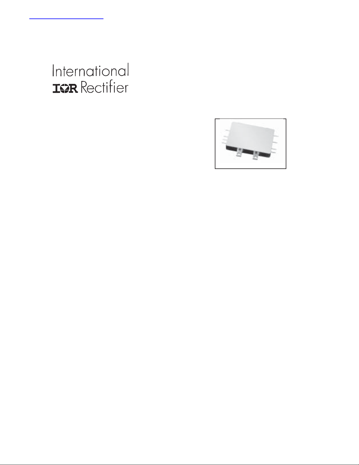
and have an adjustable output voltage. They are enclosed in a hermetic 1.5" x 2.3" x 0.425" steel package
and weigh less than 85 grams. The package utilizes
rugged ceramic feed-through copper core pins and is
sealed using parallel seam welding.
Full environmental screening includes temperature cycling, constant acceleration, fine and gross leak, and
burn-in.
Non-flight versions of the L-Series converters are available for system development purposes. Variations in
electrical specifications and screening to meet custom
requirements can be accommodated.
+ 28V Input, Single/Dual Output
Features
n Total Dose > 25K Rad(Si)
n SEE > 37 MeV.cm
n Internal EMI filter; Converter Capable of
meeting MIL-STD-461C CE03 and CS01
n Low Weight, < 85 grams
n Magnetically Coupled Feedback
n 16V to 50V DC Input Range
n Up to 25W Output Power
n Single and Dual Output Models Include
3.3, 5, 12, 15,
n High Efficiency - to 82%
n -55°C to +125°C Operating Temperature
Range
n 100M
n Under-Voltage Lockout
n Short Circuit and Overload Protection
n Output Over Voltage Limiter
n Adjustable Output Voltage
n External Inhibit
n 1,500,000 Hour MTBF
Ω @ 500VDC Isolation
2
/mg
±5, ±12 and ±15V
Applications
n Low Earth Orbit Satellites (LEO)
n Launch Vehicles
www.irf.com 1
08/20/02

L-SERIES
Circuit Description
The L-Series converters utilize a single-ended forward topology with resonant reset. The nominal
switching frequency is 500kHz. Electrical isolation
and tight output regulation are achieved through the
use of a magnetically coupled feedback. Voltage
feed-forward with duty factor limiting provides high
line rejection and protection against output over voltage in the event of an internal control loop failure.
This mechanism limits the maximum output voltage
to approximately 20% over the nominal regardless of
the line voltage.
An internal EMI filter allows the converter to meet the
conducted emissions requirements of MIL-STD-461C
on the input power leads. A single-stage output filter
reduces the typical output ripple to less than 50mV
peak-to-peak.
Output current is limited under any load fault condition to approximately 125% of rated. An overload
condition causes the converter output to behave like
a constant current source with the output voltage dropping below nominal. The converter will resume normal operation when the load current is reduced below the current limit point. This protects the converter
from both overload and short circuit conditions. The
current limit point exhibits a slightly negative temperature coefficient to reduce the possibility of thermal runaway.
An external inhibit port is provided to control converter operation. The converter’s operation is inhibited when this pin is pulled low. It is intended to be
driven by an open collector logic device. The pin
may be left open for normal operation and has a
nominal open circuit voltage of 10.5V with respect to
the input return (pin 2).
The output voltage of all models can be adjusted
using a single external resistor.
Design Methodology
The L-Series was developed using a proven conservative design methodology which includes selecting radiation tolerance and established reliability components and fully derating to the requirements
of MIL-STD-975 and MIL-STD-1547. Heavy derating of the power MOSFET gate and drain voltages
minimize the possibility of SEGR and SEB. A magnetic feedback circuit is utilized instead of opto-couplers to minimize temperature, radiation and aging
sensitivity. PSPICE was used extensively to predict
and optimize circuit performance for both beginning
and end-of-life. Thorough design analyses include
Radiation Susceptibility ( TREE ), Stress, Ther mal,
and Reliability ( MTBF ).
2 www.irf.com
L-SERIES
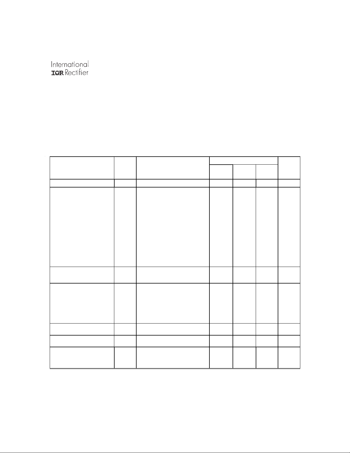
Absolute Maximum Ratings Recommended Operating Conditions
Input voltage range - -0.5Vdc to +60Vdc Input voltage range - 16Vdc to +60Vdc
Output power - Internally limited Input voltage range
1
- 16Vdc to +38Vdc
Lead temperature - +300°C for 10 seconds Output power - 0 to Max. Rated
Operating temperature - -55°C to +135°C Operating temperature
Storage temperature - -55°C to +135°C Operating temperature
1
Meets derating per MIL-STD-975
2
For operation at +125°C see table note 13
2
- -55°C to +125°C
1
- -55°C to +70°C
Electrical Performance Characteristics
Input Voltage 18 28 50 V
Output Voltage ( Vout )
Output power ( P
Output current ( I
Line regulation ( VR
Load regulation ( VR
Cross regulation ( VR
Parameter
M3L2803R3S
M3L2805S
M3L2812S
M3L2815S
M3L2805D
M3L2812D
M3L2815D
M3L2803R3S
M3L2805S
M3L2812S
M3L2815S
M3L2805D
M3L2812D
M3L2815D
)
M3L2803R3S
M3L2803R3S
OUT
All Others
OUT
M3L2805S
M3L2812S
M3L2815S
M3L2805D
M3L2812D
M3L2815D
M3L2805D
M3L2812D
M3L2815D
)
LINE
LOAD
CROSS
) 1,2,3 VIN = 16, 28, 50 Volts
Group A
Subgroup
) 1,2,3 I
)
1
1
1
1
1
1
1
2,3
2,3
2,3
2,3
2,3
2,3
2,3
1,2,3
1,2,3
1,2,3
Conditions
-55°C ≤ T
VIN = 28V DC ± 5%, CL = 0
unless otherwise specified
I
OUT
I
OUT
VIN = 16, 28, 50 Volts, Note 2
VIN = 16, 28, 50 Volts, Note 2
Either Output, Note 3
Either Output, Note 3
Either Output, Note 3
I
= 0, 50%, 100% rated, Note 4
OUT
= 0, 50%, 100% rated, Note 4
OUT
VIN = 16, 28, 50 Volts
VIN = 16, 28, 50 Volts
Duals only, Note 5
≤ +85°C
C
= 100% rated load
Note 4
= 100% rated load
Note 4
±11.88
±14.85
±11.76
±14.70
Min
3.27
4.95
11.88
14.85
±4.95
3.23
4.90
11.76
14.70
±4.90
0
0
0
0
0
0
0
0
0
-0.5
-1.0
-5.0
-3.0
-3.0
Limits
±12.00
±15.00
Nom
3.30
5.00
12.00
15.00
±5.00
12.12
15.15
±5.05
±12.12
±15.15
12.24
15.30
±5.10
±12.24
±15.30
Max
3.33
5.05
3.37
5.10
20
25
6.06
5.00
2.08
1.67
4.00
1.67
1.33
0.5 %
1.0 %
5.0
3.0
3.0
Unit
V
V
V
V
V
V
V
V
V
V
V
V
V
V
W
W
A
A
A
A
A
A
A
%
%
%
For Notes to Specifications, refer to page 5
www.irf.com 3
L-SERIES
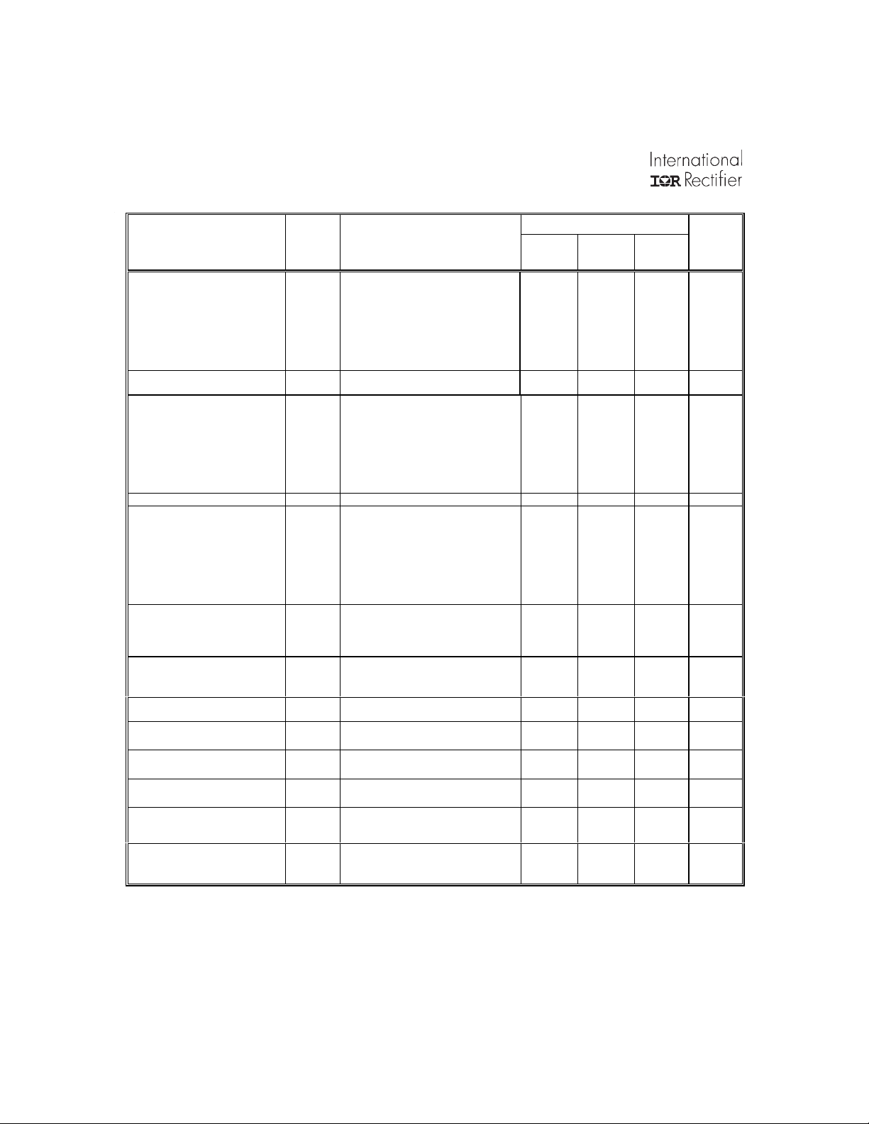
Electrical Performance Characteristics ( continued )
Parameter
Input current, no load ( IIN )
M3L2803R3S
M3L2805S
Group A
Subgroup
1,2,3
Conditions
-55°C ≤ T
V
= 28V DC ± 5%, CL = 0
IN
unless otherwise specified
I
OUT
≤ +85°C
C
= 0, Pin 4 open
M3L2812S
M3L2815S
M3L2805D
M3L2812D
M3L2815D
Input current inhibited 1,2,3 Pin 4 shorted to pin 2
Output ripple ( V
M3L2803R3S
M3L2805S
M3L2812S
)
RIP
1,2,3
V
= 16, 28, 50 Volts
IN
= 100% rated load
I
OUT
Notes 4, 6
M3L2815S
M3L2805D
M3L2812D
M3L2815D
Switching frequency ( FS ) 1,2,3 Sync. Input (Pin 4) open 425 500 575 KHz
Efficiency ( EFF )
M3L2803R3S
M3L2805S
1,2,3
I
= 100% rated load
OUT
Note 4
M3L2812S
M3L2815S
M3L2805D
M3L2812D
M3L2815D
Enable Input ( Inhibit Function )
open circuit voltage
1,2,3
Note 1 9.5
drive current ( sink )
voltage range
Current Limit Point
Expressed as a percentage
1,2,3 V
= 90% of Nominal, Note 4 105
out
of full rated load current
Power dissipation, load fault (PD) 1,2,3 Short Circuit, Overload, Note 8
Output response to
step load changes (V
Recovery time,
step load changes (T
Output response to
step line changes (V
Recovery Time,
step line changes (T
Turn-on Response
Overshoot (V
Turn-on Delay (T
TLN
TLN
TLD
TLD
)
)
)
)
)
OS
)
DLY
4,5,6 Half Load to/from Full Load, Notes 4,9 -300
4,5,6 Half Load to/from Full Load, Note
4,9,10
4,5,6 16V to/from 50V
I
= 100% rated load, Notes 1,4,11
OUT
4,5,6 16V to/from 50V
I
= 100% rated load, Notes
OUT
4,5,6
1,4,10,11
No Load, Full Load
Notes 4,12
Min
68
75
75
75
75
75
75
-0.5
-300
Limits
Nom
75
79
80
81
79
79
80
2
Max
60
70
70
70
70
100
100
8 mA
35
50
70
80
80
80
80
11.5
500
50
130 %
14 W
300 mV pk
200
300 mV pk
200
500
10
Unit
mV p-p
mV p-p
mV p-p
mV p-p
mV p-p
mV p-p
mV p-p
mA
mA
mA
mA
mA
mA
mA
%
%
%
%
%
%
%
V
µ
V
µ
µ
mV
mS
A
S
S
For Notes to Specifications, refer to page 5
4 www.irf.com

L-SERIES
Electrical Performance Characteristics
Parameter
Capacitive Load (CL)
M3L2803R3S
Group A
Subgroup
1
M3L2805S
M3L2812S
M3L2815S
M3L2805D
M3L2812D
M3L2815D
Line Rejection 1 I
Isolation 1 Input to Output or Any Pin to Case
Device Weight
MTBF
V
unless otherwise specified
No effect on DC performance
except pin 3, test @ 500VDC
MIL-HDBK-217F2, SF, 35°C
( continued )
Conditions
-55°C ≤ T
= 28V DC ± 5%, CL = 0
IN
I
OUT
Each output on duals
OUT
DC to 50KHz, Notes 1, 4
≤ +85°C
C
= 100% rated load
Notes 1, 4, 7
= 100% rated load
40 50
100
1.5 x 10⁶
Limits
2200
1000
180
120
500
90
60
85 grams
Table I. Electrical Performance Characteristics - notes
1) Parameter is tested as part of design characterization or after design changes. Thereafter, parameter shall be guaranteed to the
limits specified.
2) Parameter verified during line and load regulation tests.
3) Output load current must be distributed such that at least 20% of the total load current is being provided by one of the outputs.
4) Load current split equally between outputs on dual output models.
5) Cross regulation is measured with 20% rated load on output under test while changing the load on the other output from 20% to 80%
of rated.
6) Guaranteed f or a D.C. to 20MHz bandwidth. Tested using a 20KHz to 10MHz bandwidth using the circuit shown below.
7) Capacitive load may be any value from 0 to the maximum limit without compromising dc performance. A capacitive load in excess
of the maximum limit may interfere with the proper operation of the converter’s overload protection, causing erratic behavior during
turn-on.
8) Overload power dissipation is defined as the device power dissipation with the load set such that V
9) Load step transition time ≤ 10 µSec.
10) Recovery time is measured from the initiation of the transient to where V
its steady state value.
11) Line step transition time ≤ 100 µSec.
12) Turn-on delay time from either a step application of input power or a logic low to a logic high transition on the inhibit pin (pin 4) to
the point where V
13) For operation at temperatures between +85°C and +125°C, derate the maximum output power linearly from 100% to 75%.
= 90% of nominal.
OUT
has returned to within ±1% of
OUT
= 90% of nominal.
OUT
Unit
µF
µF
µF
µF
µF
µF
µF
dB
MΩ
Hours
www.irf.com 5

L-SERIES
Radiation Performance Characteristics
Highest
Total Ionizing Dose ( Gamma ) MIL-STD-883, Method 1019
Single Event Effects
SEU, SEL, SEGR, SEB
Dose Rate ( Gamma Dot )
Neutron Fluence MIL-STD-883, Method 1017 3E12 8E12 Neutrons
Proton Fluence E > 10MeV TBD N/A protons
Test
Temporary Saturation
Survival
Operating bias applied during exposure,
Operating bias applied during exposure,
Operating bias applied during exposure,
Conditions
Full Rated Load, V
Heavy ions (LET)
Full Rated Load, V
MIL-STD-883, Method 1023
Full Rated Load, VIN = 28V
= 28V
IN
= 28V
IN
Min Typ
25 40 60 KRads
37 82 82
1E8
1E10
Level
Tested Unit
1.5E9 Rads
Device Screening
Test Inspection
Element Evaluation
Nondestructive Bond Pull
Internal Visual
Temperature Cycling
Constant Acceleration
Electrical
Burn-in
Final Electrical ( Group A )
Seal
Fine Leak
Gross Leak
External Visual
Method
MIL-PRF-38534 class H equivalent with SEM
MIL-STD-883, Method 2023
MIL-STD-883, Method 2017
MIL-STD-883, Method 1010
MIL-STD-883, Method 2001 (2k-g)
In accordance with
device specification
MIL-STD-883, Method 1015
In accordance with
device specification
MIL-STD-883, Method 1014
MIL-STD-883, Method 2009
Condition
C
A, Y1 axis only
160 Hours
A1
C
(Si)
MeV•cm
/mg
(Si)/sec
/cm2
/cm
2
2
6 www.irf.com

L-SERIES
INHIBIT
RETURN
CASE
GROUND
Vin
1
4
2
3
EMI
FILTER
RAMP
GEN.
BIAS
SUPPLY
+10.5V
PWM
CONTROLLER
SAMPLE
&
HOLD
FEEDBACK
TRIGGER
7Vin
+OUTPUT
OUTPUT
6
RETURN
+
EA
-
OUTPUT
5
ADJUST
Block Diagram - Single Output
1
EMI
FILTER
8 +OUTPUT
7
RETURN
INHIBIT
RETURN
CASE
GROUND
+10.5V
RAMP
GEN.
BIAS
SUPPLY
PWM
CONTROLLER
SAMPLE
&
HOLD
FEEDBACK
TRIGGER
+
EA
-
4
2
3
6 -OUTPUT
OUTPUT
5
ADJUST
Block Diagram - Dual Output
www.irf.com 7

L-SERIES
y
y
100
90
80
70
60
50
dB-uA
40
30
20
10
0
1E3 1E4 1E5 1E6 1E7 1E8
Frequenc
CEO3 LIMIT
( Hz )
Conducted Emissions, Common Mode
100
90
80
70
60
50
dB-uA
40
CEO3 LIMIT
30
20
10
0
1E3 1E4 1E5 1E6 1E7 1E8
Frequenc
( Hz )
Conducted Emissions, Normal Mode
8 www.irf.com

0
-10
-20
-30
-40
-50
dB
-60
-70
-80
-90
-100
1E2 1E3 1E4 1E5
Frequency ( Hz )
M3L2805S Line Rejection (CS01)
L-SERIES
0
-10
-20
-30
-40
-50
dB
-60
-70
-80
-90
-100
1E2 1E3 1E4 1E5
Frequency ( Hz )
M3L2815D Line Rejection (CS01)
www.irf.com 9

L-SERIES
5
ply
0
-10
-20
-30
-40
-50
dB
-60
-70
-80
-90
-100
1E2 1E3 1E4 1E
M3L2815D Line Rejections (CS01)
Frequency ( Hz )
1 µF
Ω
50
T erm in a t ion
Oscilliscope or Equivalent
with 10 MHz Bandwidth.
readings by 2.
Multi
DUT
+ Vout
Return
0.1 µF
Ω
Ω
50
RL for I
Coax50
RATED
Circuit for Measuring Output Ripple Voltage
10 www.irf.com

2.300
g
1.5500.375
0.25 Typ.
Mechanical Diagram
ø 0.128
4 P lcs
L-SERIES
0.050
0.470
0.400
2 Eq Spaces
@ 0.200
1423
0.250
0.8500.350
2.80
Ref
Pin Designation (Single/Dual)
Pin Number Single Dual
Pin 1 + Input + Input
Pin 2 Input Return Input Return
Pin 3 Case Case
Pin 4 Inhibit Inhibit
Pin 5 Output Adjust Output Adjust
Pin 6 Output Return - Vout
Pin 7 + Vout Output Common
Pin 8 NC + Vout
8
76
1.500 1.750 2.000
5
0.425
Max
M3L 28 05 S
Model
Input Volta
28 = 28V Nominal
0.270
1.000
Ref
Pin ø
0.040
0.220
To le ra n ce : .XX = ±0 .0 1
.XX X = ±0 .0 0 5
Part Number
e
Output Voltage
03R3 = 3.3V, 05 = 5V
12 = 12V, 15 = 15V
0.400
0.400
0.200
Outputs
S = Single
D = Dual
WORLD HEADQUARTERS: 233 Kansas St., El Segundo, California 90245, Tel: (310) 322 3331
ADVANCED ANALOG: 2270 Martin Av., Santa Clara, California 95050, Tel: (408) 727-0500
Visit us at www.irf.com for sales contact information.
Data and specifications subject to change without notice. 02/03
www.irf.com 11
 Loading...