International Rrectifier IRSF3011 User Manual

查询IRSF3011供应商
Data Sheet No.PD 6.039B
FULLY PROTECTED POWER MOSFET SWITCH
IRSF3011
Features
· Extremely Rugged for Harsh Operating Environments
· Over-Temperature Protection
· Over-Current Protection
· Active Drain-to-Source Clamp
· ESD Protection
· Compatible with Standard Power MOSFET
· Low Operating Input Current
· Monolithic Construction
Description
The IRSF3011 is a three-terminal monolithic Smart Power MOSFET
with built-in short circuit, over-temperature, ESD and over-voltage protections.
The on-chip protection circuit latches off the power MOSFET in case
the drain current exceeds 7A or the junction temperature exceeds 165°C
and keeps it off until the input is driven low. The drain-to-source voltage
is actively clamped at 55V (typical), prior to the avalanche of POWER
MOSFET, thus improving its performance during turn-off with inductive
loads.
The input current requirements are very low (300µA) which makes the
IRSF3011 compatible with most existing designs based on standard
power MOSFETs.
V
ds(clamp)
R
ds(on)
I
ds(sd)
T
j(sd)
E
AS
Applications
· Solenoid Driver
· DC Motor Driver
Available Packages
IRSF3011
(TO-220AB)
IRSF3011L
(SOT-223)
50V
200mΩ
5A
155°C
200mJ
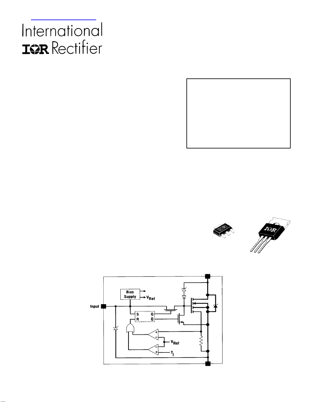
IRSF3011 Block Diagram

IRSF3011
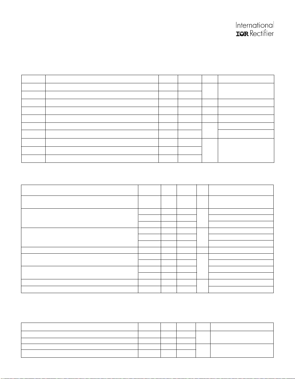
Absolute Maximum Ratings
Absolute Maximum Ratings indicate sustained limits beyond which damage to the device may occur. (Tc = 25°C unless
otherwise specified.)
Minimum Maximum Units Test Conditions
V
ds, max
V
in, max
I
ds
P
d
E
AS
V
esd1
V
esd2
T
Jop
T
Stg
T
L
Static Electrical Characteristics
(Tc = 25°C unless otherwise specified.)
V
ds,clamp
R
ds(on)
I
dss
V
th
I
i,on
I
i, off
V
in, clamp
V
sd
Continuous Drain to Source Voltage 50
Continuous Input Voltage -0.3 10
Continuous Drain Current self limited
Power Dissipation 30 W T
Unclamped Single Pulse Inductive Energy➁ 200 mJ
Electrostatic Discharge Voltage (Human Body Model) 4000
Electrostatic Discharge Voltage (Machine Model) 1000 200pF, 0Ω
Operating Junction Temperature Range -55
Storage Temperature Range -55 175 °C
Lead Temperature (Soldering, 10 seconds) 300
self-limited
V
V
≤ 25°C
c
1000pF. 1.5kΩ
Minimum Typical Maximum Units Test Conditions
Drain to Source Clamp Voltage 50 54
5662 Ids = 6A, tp = 700 µS
Drain to Source On Resistance 155 200 Vin = 5V, Ids = 2A
200 mΩ V
115 Vin = 10V, Ids = 2A
Drain to Source Leakage Current 10 Vds = 12V, Vin = 0V
100 µA Vds = 50V, Vin = 0V
10 250 Vds=40V,Vin=0V,Tc=150°C
Input Threshold Voltage 1.5 2.0 2.5 V V
Input Supply Current (Normal Operation) 0.25 0.6 Vin = 5V
0.35 0.85
Input Supply Current (Protection Mode) 0.5 1.0 Vin = 5V
0.6 1.2 Vin = 10V
Input Clamp Voltage 10 10.8
Body-Drain Diode Forward Drop➂ 1.2 1.5 I
V
mA
V
Ids = 10mA
= 4V, Ids = 2A
in
= 5V, Ids = 10mA
ds
Vin = 10V
Iin = 10mA
= -9A, R
ds
= 1kΩ
in
Thermal Characteristics
RΘ
RΘ
RΘ
RΘ
2
Junction to Case 4
jc
Junction to Ambient 62
jA
Junction to PCB 40
jc
Junction to PCB ➀ 60
jA
Minimum Typical Maximum Units Test Conditions
°C/W TO-220AB
°C/W SOT-223

IRSF3011
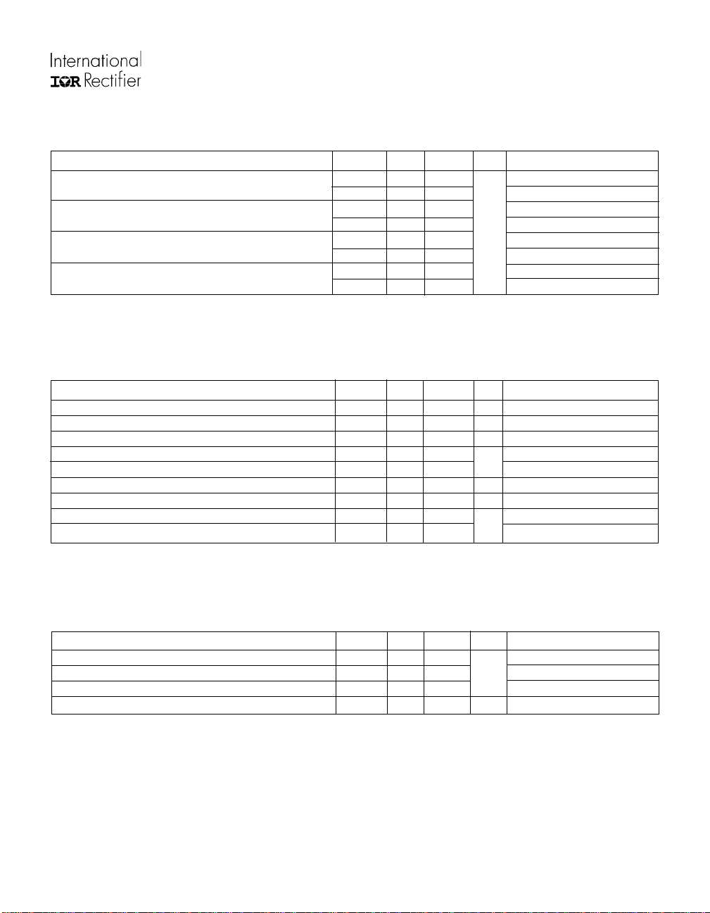
Switching ElectricalCharacteristics
(VCC = 14V, Resistive Load (RL) = 5Ω, TC= 25°C.) Please refer to Figure 15 for switching time definitions.
Minimum Typical Maximum Units Test Conditions
t
don
t
r
t
doff
t
f
Protection Characteristics
(TC= 25 °C unless otherwise specified.)
I
ds(sd)
T
j(sd)
V
protect
t
Iresp
t
Iblank
I
peak
V
reset
t
reset
t
Tresp
Turn-On Delay Time 160 250 Vin = 5V
90 Vin = 10V
Rise Time 650 1200 Vin = 5V
250
Turn-Off Delay Time 250 350 Vin = 5V
300 Vin = 10V
Fall Time 180 350 Vin = 5V
170 Vin = 10V
nS
Vin = 10V
Minimum Typical Maximum Units Test Conditions
Over-Current Shutdown Threshold 5 7 10 A Vin = 5V
Over Temperature Shutdown Threshold 155 165 °C Vin = 5V, Ids = 2A
Min. Input Voltage for Over-temp function 3 V
Over Current Response Time 4
Over Current Blanking Time 4 See Figure 16 for definition
Peak Short Circuit Current 16 A See Figure 16 for definition
Protection Reset Voltage 1.3 V
Protection Reset Time 8
Over-Temperature Response Time 12 See Figure 18 for definition
See Figure 16 for definition
µS
See Figure 17 for definition
µS
Temperature Coefficients of Electrical Characteristics
(Please see Figures 3 through 14 for more data on thermal characteristics of other electrical parameters.
Minimum Typical Maximum Units Test Conditions
V
ds,clamp
V
th
V
in,clamp
I
ds(sd)
Notes:
① When mounted on a 1" square PCB (FR-4 or G10 material). For recommended footprint and soldering techniques, refer
to International Rectifier Application Note AN-994.
② E
③ Input current must be limited to less than 5mA with a 1kΩ resistor in series with the input when the Body-Drain Diode
is forward biased.
Drain-to-Source Clamp Voltage T.C. 18.2 Ids = 10mA
Input Threshold Voltage T.C. -2.7 mV/°C Vds = 5V, Ids = 10mA
Input Clamp Voltage T.C. 7.0 Iin = 10mA
Over-Current Shutdown Threshold T.C. -9.8 mA/°C Vin = 5V
is tested with a constant current source of 6A applied for 700µS with Vin = 0V and starting Tj = 25°C.
AS
3

IRSF3011
I
)
R
)
Vin = 5V
Vin = 8V
Vin = 10V
I
s)
S
)
T = 25°C
T
)
R
)
Vin = 10V
Ids = 4A
Vin = 5V
T
)
S
)
Vin = 5V
250
T = 25°C
225
200
175
150
ds(on) (mOhm
125
100
12345678
Vin = 4V
ds (A
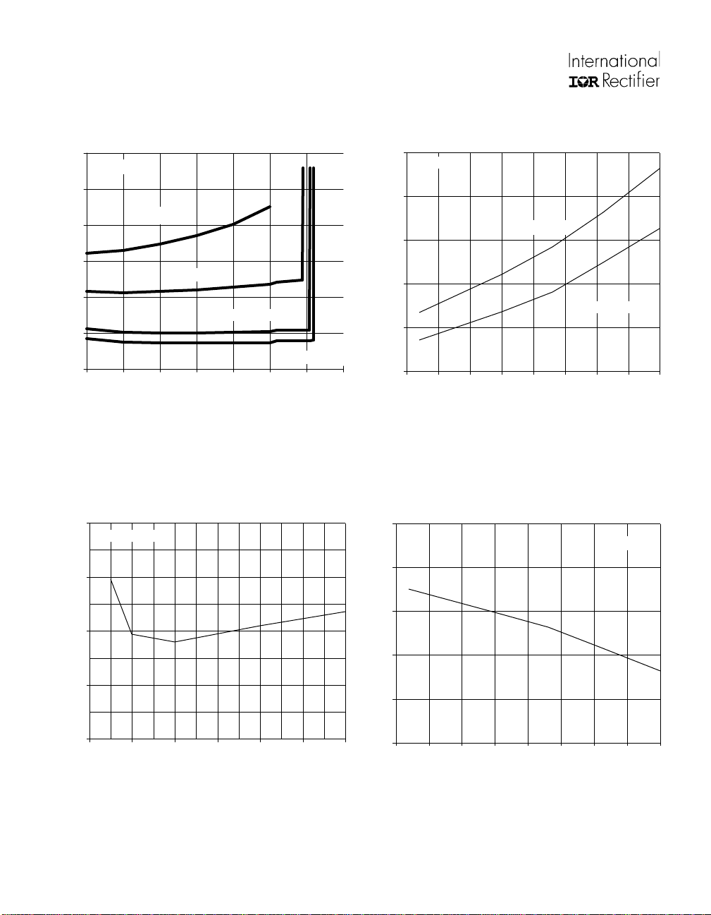
Figure 3 On Resistance vs.
Drain-to-Source Current
8
300
250
200
150
ds(on) (mOhm
100
50
-50 -25 0 25 50 75 100 125 150
emperature (°C
Figure 4 On Resistance vs. Temperature
9
7.5
7
hut Down Current (A
6.5
6
45678910
nput V o l tage ( Vo l t
Figure 5 Over-Current Shutdown Threshold vs.
Input Voltage
4
8
7
6
hut Down Current (A
5
4
-50 -25 0 25 50 75 100 125 150
emperature (°C
Figure 6 Over-Current Shutdown Threshold vs.
Temperature
 Loading...