International Rrectifier IRSF3010 User Manual

查询IRSF3010供应商
Provisional Data Sheet No.PD-6.0027A
IRSF3010
FULLY PROTECTED POWER MOSFET SWITCH
Rating Summary:General Description:
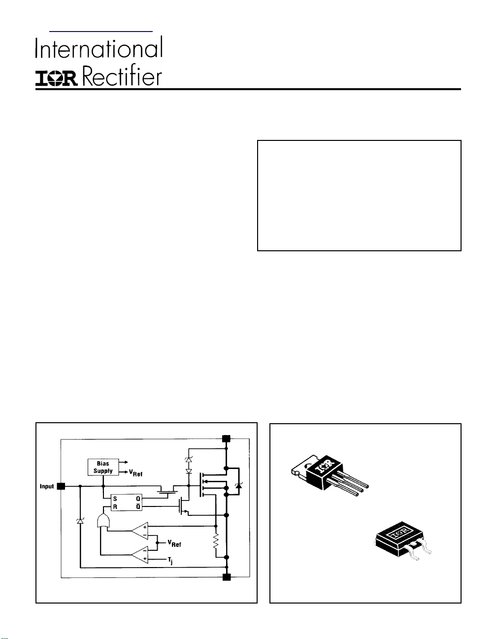
The IRSF3010 is a three terminal monolithic
SMART POWER MOSFET with built in short circuit, over-temperature, ESD and over-voltage protections.
The on chip protection circuit latches off the
POWER MOSFET in case the drain current exceeds 14A (typical) or the junction temperature exceeds 165°C (typical) and keeps it off until the
input is driven low. The drain to source voltage
is actively clamped at 55V (typical), prior to the
avalanche of POWER MOSFET, thus improving
its performance during turn off with inductive
loads.
The input current requirements are very low
(300uA) which makes the IRSF3010 compatible with
most existing designs based on standard
POWER MOSFETs.
Applications:
n DC Motor Drive
n Solenoid Driver
Drain
V
ds(clamp)
R
ds(on)
I
ds(sd)
T
j(sd)
E
AS
50 V
80 m
11 A
155 °C
400 mJ
Features:
n Extremely Rugged for Harsh Operating
Environments
n Over Temperature Protection
n Over Current Protection
n Active Drain to Source Clamp
n ESD Protection
n Compatible with standard POWER
MOSFET
n Low Operating Input Current
n Monolithic Construction
n Dual set/reset Threshold Input
Pin Assignment
Pin 1 - Input
3
2
1
Pin 2 - Drain
Pin 3 - Source
Tab - Drain
Tab
IRSF3010
ΩΩ
Ω
ΩΩ
Source
IRSF3010S
Available PackagesIRSF3010 - Block Diagram

IRSF3010
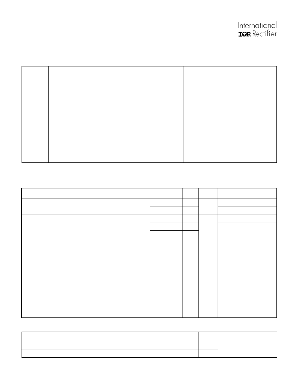
Absolute Maximum Ratings
Absolute Maximum Ratings indicate sustained limits beyond which damage to the device may occur. (Tc =
25°C unless otherwise specified.)
Symbol Parameter Definition Min. Max. Test Conditions
V
V
I
ds
P
E
V
V
T
T
T
L
ds, max
in, max
d
AS
esd1
esd2
Jop
Stg
Continuous Drain to Source Voltage — 50
Continuous Input Voltage -0.3 10
Continuous Drain Current — self limited
Power Dissipation — 40 W T
Linear Derating Factor for Tc > 25°C — 0.33 W/°C
Unclamped Single Pulse Inductive Energy — 40 0 mJ
Electrostatic Discharge Voltage (Human Body Model) — 4000 1000pF . 1.5kΩ
(Machine Model) — 1000 200pF, 0Ω
Junction T emperature -55
Storage T emperature -55 175
Lead T emperature (Soldering, 10 seconds) — 300
self-limited
Static Electrical Characteristics
(Tc = 25°C unless otherwise specified.)
Symbol Parameter Definition Min. Typ. Max. Units Test Conditions
V
ds,clamp
R
ds(on)
I
dss
V
th
I
i, on
I
i, off
V
in, clamp
V
sd
Drain to Source Clamp Voltage 50 54 — Ids = 10mA
—5662 Ids = 11A, tp = 700 µS
Drain to Source On Resistance — 70 80 Vin = 5V, Ids = 4A
—85— Vin = 4V, Ids = 4A
—53— Vin = 10V, Ids = 4A
Drain to Source Leakage Current — — 10 Vds = 12V, Vin = 0V
— — 100 Vds = 50V, Vin = 0V
— 10 250 V
Input Threshold Voltage 1.5 2.0 2.5 V Vds = 5V, Ids = 1mA
Input Supply Current (Normal Operation) — 0.25 0.6 Vin = 5V
— 0.35 0.85 Vin = 10V
Input Supply Current (Protection Mode) — 0.5 1.0 Vin = 5V
—0.61.2 Vin = 10V
Input Clamp Voltage 10 10.8 — Iin = 10mA
Body-Drain Diode Forward Drop ➁ — 1.2 1.5 Ids = -17A, Rin = 1k
Units
V
mΩ
µA
mA
V
V
≤ 25°C
c
V
o
C
=40V,Vin=0V,Tc=150oC
ds
Ω
Thermal Characteristics
Symbol Parameter Definition Min. Typ. Max. Units Test Conditions
R
Θjc
R
ΘjA
2
Thermal Resistance, Junction to Case — 3 . 0 — °C/W
Thermal Resistance, Junction to Ambient — 6 0 — °C/W

IRSF3010
Switching Electrical Characteristics:
(Vcc = 14V, Resistive Load RL = 5Ω, Tc = 25 °C.) Please refer to Figure 15 for switching time definitions.
Symbol Parameter Definition Min. Typ. Max. Units Test Conditions
t
don
t
r
t
doff
t
f
Protection Characteristics:
(Tc = 25 °C unless otherwise specified.)
Symbol Parameter Definition Min. Typ. Max. Units Test Conditions
I
ds(sd)
T
j(sd)
V
protect
t
Iresp
t
Iblank
I
peak
V
reset
t
reset
t
Tresp OverTemperature Response Time
Turn-On Delay time — 4 25 650 Vin = 5V
— 150 — Vin = 10V
Rise Time — 2000 4000 Vin = 5V
— 425 — Vin = 10V
Turn-Off Delay time — 650 1000 Vin = 5V
— 850 — Vin = 10V
Fall Time — 5 0 0 800 Vin = 5V
— 450 — Vin = 10V
Over-Current Shutdown Threshold 11 14 17 A Vin = 5V
Over Temperature Shutdown Threshold 155 165 — °C Vin = 5V, Ids = 2A
Minimum Input Voltage for Over-temp fxn. — 3 — V
Over Current Response Time — 2 — See figure 16 for definition
Over Current Blanking Time — 3 — See figure 16 for definition
Peak Short Circuit Current — 20 — A See figure 16 for definition
Protection Reset Voltage — 1.3 — V
Protection Reset Time — 7 — See figure 17 for definition
— 12 — See figure 18 for definition
nS
µS
µS
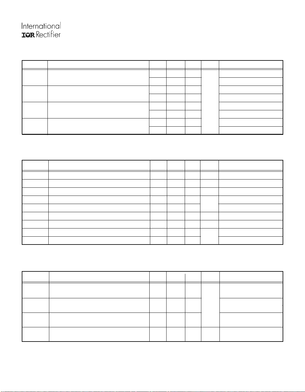
T emperature Coefficients of Electrical Characteristics:
(Please see Figures 3 through 14 for more data on thermal characteristics of other electrical parameters.
Symbol Parameter Definition Min. Typ. Max. Units Test Conditions
V
ds,clamp
V
th
V
in,clamp
I
ds(sd)
Notes:
1. EAS is tested with a constant current source of 11A applied for 700µS with Vin = OV and starting Tj = 25oC.
2. Input current must be limited to less than 5mA with a 1kΩ resistor in series with the input when the Body-Drain Diode
is forward biased.
Temperature Coefficient of Drain to Source
Clamp Voltage — 18.2 —
Temperature Coefficient of Input Threshold
Voltage — -3.2 —
Temperature Coefficient of Input Clamp
Voltage — 7.0 —
Temperature Coefficient of Over-Current
Shutdown Threshold — -21.5 — mA/oC
mV/oC
Ids = 10mA
Vds = 5V, Ids = 1mA
Iin = 10mA
Vin = 5V
3

IRSF3010
120
T = 25°C
110
100
90
80
70
Rds(on) (mOhm)
60
50
40
24681012141618
Vin = 4V
Vin = 5V
Vin = 7V
Vin = 10V
Ids (A)
120
110
100
90
80
70
60
Rds(on) (mOhm)
50
40
30
Ids = 4A
Vin = 5V
Vin = 10V
-50 -25 0 25 50 75 100 125 150
Temperature (°C)
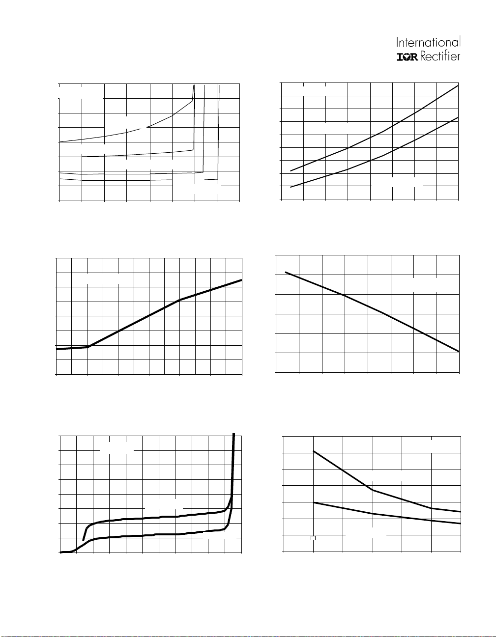
Fig. 3 - On Resistance vs Drain to Source Current Fig. 4 - On Resistance vs. Temperature
17
16
15
14
Shut Down Current (A)
T = 25°C
16
15
14
13
12
Shut Down Current (A)
11
Vin = 5V
13
45678910
Input Voltage (Volts)
Fig. 5 - Over-current Shutdown Threshold vs
Input Voltage
1.6
1.4
1.2
1
0.8
0.6
0.4
Input Current (mA)
0.2
0
01234567891011
T=25°C
Iin,of f
Iin,on
Input Voltage (Volt s )
Figure 7 - Input Current vs. Input Voltage
4
10
-50 -25 0 25 50 75 100 125 150
Temperature (°C)
Fig. 6 - Over-current Shutdown Threshold vs
Temperature
3500
3000
2500
2000
1500
1000
500
Single Pulse Energy to Failur e (mJ)
0
0255075100125150
Rating
Starting Junc tion Temperature (°C)
Ids = 8A
Ids = 12A
Vdd = 25V
Fig. 8 - Unclamped Single Pulse Inductive Energy to
Failure vs Starting Junction Temperature
 Loading...