


IRPLCFL8U
Simplified Three Level Dimming CFL Fluorescent
Ballast using the IRS2530D DIM8
Table of Contents
1. Features ...........................................................................................2
TM
Page
2. Overview ..........................................................................................2
3. Circuit Schematic ............................................................................. 8
4. Electrical Characteristics ..................................................................9
5. Fault Protection Characteristics ....................................................... 9
6. Functional Description....................................................................10
7. Fault Conditions .............................................................................15
8. Ballast Design ................................................................................19
9. Bill of Materials...............................................................................22
10. IRPLCFL8U PCB Layout..............................................................23
11. Inductor Specifications .................................................................27
www.irf.com
RD0803
- 1 -
1. Features
Drives 1 x 32W Spiral CFL Lamp
Input Voltage: 120Vac
High Frequency Operation
Lamp Filament Preheating
Lamp Fault Protection with Auto-Restart
Low AC Line/Brownout Protection
IRS2530D DIM8TM HVIC Ballast Controller
2. Overview
The 3 way dimming system widely adopted in the US with conventional filament lamps
consists of a light bulb that has a modified Edison screw type base which allows 3
connections to be made to a special lamp socket that also has 3 connections.
Standard Edison Screw
Base
Live
Neutral
Figure 2.1: Three way dimming Edison screw base
The 3 way dimming light bulb has two filaments inside which produce different light
outputs when connected to the AC line. These filaments are connected in series such that
the mid point goes to the line common and the two ends can be connected to the live
3 Way Dimming Edison
Screw Base
Live 1 Live 2
Neutral
www.irf.com
RD0803
- 2 -
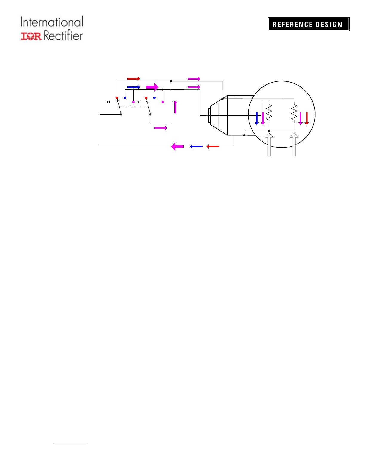
either independently or both together. Thus with an external switch that has four positions,
it is possible to obtain 3 different light levels or to switch off.
3 Way Dimming Switch
3 Way Dimming Light Bulb
Live
120V AC Line
Neutral
1 2
0
Figure 2.2: Three way dimming filament lamp system
3 0
1 2
3
40W Filament60W Filament
Figure 2.2 shows how the live and the neutral connect for 4 different configurations
(position 0, 1, 2, and 3). The flow of current for each position is also shown with colored
arrow; no current flows for position 0 (switch off), red arrow for position 1, blue arrow for
position 2, and magenta arrow for position 3. In position 1, the current will flow through
the 40W filament resistor (the lowest dimming level). In position 2, the current will flow
through the 60W filament resistor (intermediate dimming level). In position 3, current
will flow through both filaments, and the system will be at the maximum dimming level.
Existing Ballast Solution
There are in existence CFL ballast designs that provide three way dimming based on
the same switching arrangement shown above. A common approach is a system
whereby the line voltage is full wave rectified when one live input is connected and a
voltage doubler circuit comes into operation when the other live input is connected or
both are connected together thereby having two DC bus voltages in the ballast during
dim level settings. This type of design also operates at two different frequencies, a low
frequency (typically 40-45kHz) when both live inputs are connected providing a high
lamp current and a higher frequency (for example 70-75kHz) when either of the two
lives is connected alone which will produce a lower lamp current. In this way the
following combinations are achieved:
1. Low DC bus (150V) / high frequency ….. minimum output
2. High DC bus (300V) / high frequency …... medium output
3. High DC bus (300V) / low frequency …… maximum output
This approach has some serious drawbacks:
Firstly, since the ballast must be designed to give 100% light output for the lamp when
the bus voltage is 300V and the frequency is 40kHz, it is not easy to achieve
satisfactory preheat and ignition when the bus voltage is at 150V because of the
limitations in the peak voltage that the output circuit is able to produce from a 150Vpp
half bridge voltage.
www.irf.com
RD0803
- 3 -

One strategy that has been used is to omit the preheating phase and steer the
oscillator frequency to resonance during ignition using feedback from the output circuit.
This ensures that at switch-on the highest possible ignition voltage will be applied to the
lamp. In this way the lamp will ignite in whichever position the 3 way switch is set.
Such a scheme could reliably ignite the lamp when the DC bus is at 300V, however
without correct preheating the ignition voltage of the lamp and consequently the peak
current in the MOSFET half bridge during ignition will be higher. Also the life of the
lamp is substantially reduced when there is no preheat due to far greater stress
occurring on the cathodes at the point of ignition.
Ignition when the DC bus voltage is at 150V is very difficult. Tests indicated that
sweeping the frequency down through resonance sometimes failed to produce
sufficient ignition voltage leaving the ballast in open circuit running mode. The
conclusion from this is that the ballast needs to oscillate at resonance for an extended
period of time in order for the lamp to ignite at 150V considering that the output inductor
and capacitor have been designed to produce 100% lamp power at 300VDC bus when
the frequency is 40-45kHz.
Many CFL ballast designs do not incorporate a current sense and shutdown function to
protect the circuit in the case of ignition failure and so the ballast would eventually fail if
left switched on due to the high MOSFET switching losses causing thermal destruction.
This would not matter with and integrated ballast / lamp type product when the lamp
has failed.
It has also been observed that hard switching occurs at the MOSFET half bridge when
the DC bus voltage is low in position 1 since when the ballast is running it will be close
to resonance, bearing in mind that the resonant frequency shifts downwards in run
mode. Hard switching is very undesirable because of the high peak currents that occur
when each MOSFET switches on. This has been shown to result in a higher rate of
field failures in ballasts due to MOSFET failure.
The conclusion is that the approach to design described above is unable to provide a
reliable ballast.
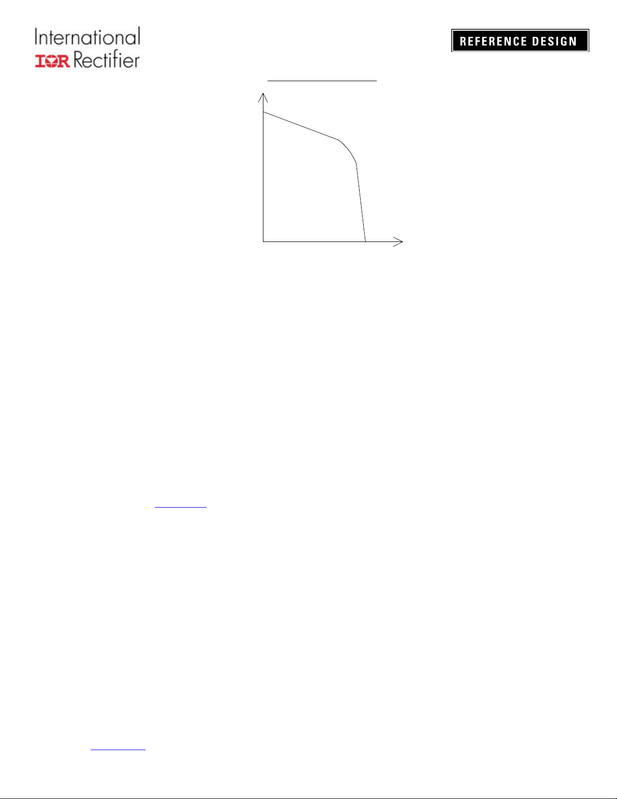
The dimming level can also be controlled by simply changing the frequency. By
changing the frequency between 3 defined settings, however, it was found to be
extremely difficult to set a point where the dim level is 50%. The problem with this is
that the lamp current against ballast frequency characteristic of the system exhibits a
very sharp knee such that as the frequency increases the lamp current is gradually
reduced up to a point at which a small increase of frequency will result in a very large
reduction in the lamp current.
www.irf.com
RD0803
- 4 -
Ballast / Lamp Operati ng Characteristic
Lamp
Current
Ballast Running
Frequency
Figure 2.3: Lamp current against ballast frequency
To obtain 50% output, the frequency would have to be very precisely set. This is not
practical since the tolerances of the output inductor, capacitor and oscillator timing
components do not allow this. Even if each ballast was individually adjusted in
production variations in lamp behavior over temperature would mean that under some
conditions the lamp arc would extinguish at this setting leaving the system in
permanent preheat which would burn out the cathodes eventually.
This explains why the 150VDC bus solution has been adopted in some designs as this
allows 50% output to be achieved without this problem. However as discussed in the
previous section this approach is not without some major disadvantages.
IRPLCFL4 Reference Design
It is however necessary in order to create a reliable design to include a closed loop
feedback system that controls the lamp current by adjusting the ballast frequency from
a VCO (voltage controlled oscillator) driven by the output of an error amplifier that
senses the lamp arc current directly and compares it with a reference. This has been
used in the IRPLCFL4 reference design “A 3 Way Dimming CFL Ballast” and has been
demonstrated to be capable of controlling the lamp output down to approximately 10%
arc current maintaining stability. This also compensates for tolerances in the
components of the circuit or the lamp.
www.irf.com
RD0803
- 5 -
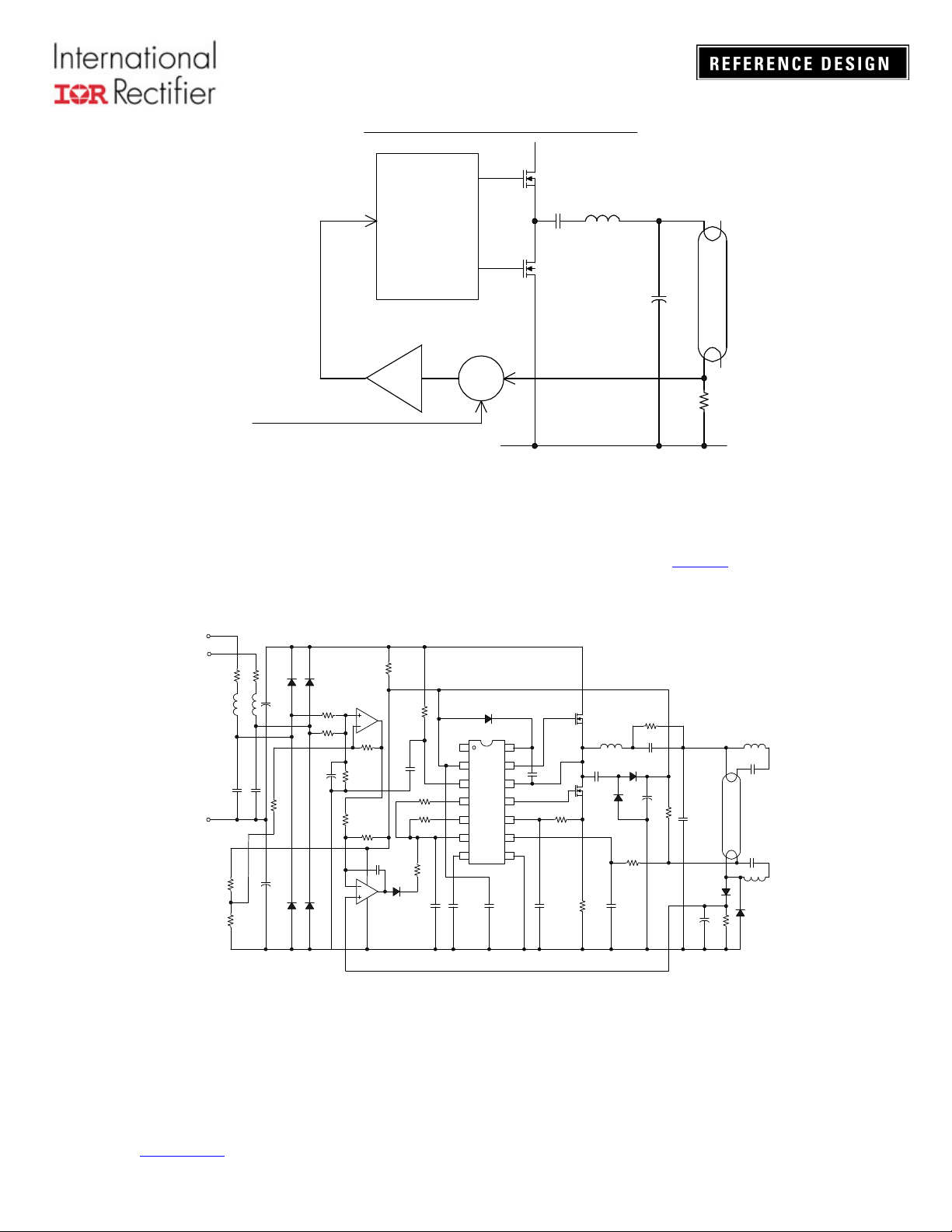
∑
Regulated Lamp Current Control System
VCO
&
DRIVER
+
Lamp Arc Current
Reference
-
Figure 2.4: Closed loop lamp arc current regulation
Many of the design issues described above have also been overcome in the ballast
circuit of reference design IRPLCFL4. The design, however, required two additional
operational amplifiers and additional circuitry since it is based on the IR2156 control IC,
which does not incorporate the necessary dimming circuitry. This circuit therefore has a
relatively high component count.
L1
L2
COMMON
R4
R5
R1
L1
C1 C2
R2
L2
D1 D2
C3
R6
C4
D3
R7
R8
C7
D4
5
6
R10
R12
2
3
IC1a
R11
R9
8
4
R3
R15
7
NC
VCC
VDC
R16
RT
R17
RPH
CT
CPH
C9 C10 C11
C8
1
IC1b
C20
D7
R18
D8
IC2
IR2156
VB
14
HO
13
VS
12
LO
11
CS
10
SD
9
COM
8
C6
1
2
3
4
5
6
7
Q1
L3
R19
C13
Q2
D10
C19
R20
C5
C14
R21
R13
C15
D9
R9
C16
C12
L3a
C17
C18
L3b
D5
D6
R14
Figure 2.5: IRPLCFL4 Circuit Schematic
The component count for the IRPLCFL4 design shown in figure 2.5 is 56 parts.
www.irf.com
RD0803
- 6 -

New Solution: IRPLCFL8U
A completely new approach has been developed that overcomes all of the above
limitations. The IRPLCFL8U reference design kit consists of a dimming Fluorescent
ballast, with a 3 way dimming switch, driving a single 32W CFL lamp. The design
contains an EMI filter and a dimming ballast control circuit using the
IRS2530D(
50 parts. This demo board is intended to help with the evaluation of the IRS2530D
dimming ballast control IC, demonstrate PCB layout techniques and serve as an aid in
the development of production ballasts using the IRS2530D.
DIM8
TM
). The component count for the IRPLCFL8U, shown in figure 3.1, is
www.irf.com
RD0803
- 7 -
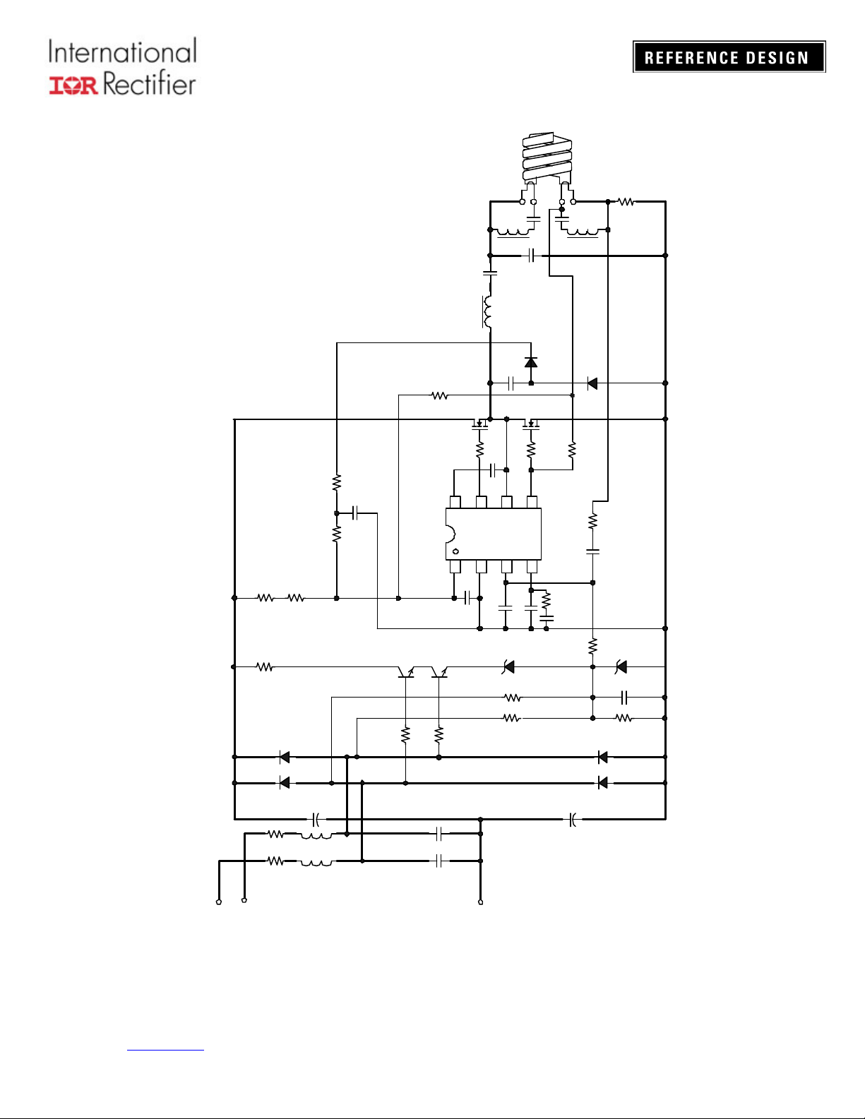
3. Circuit Schematic
SPIRAL
CFL LAMP
CH1
LRES : B
CDC
LRES:A
RLMP2
MHS
RHO
VB
HO
8
7
RVCC2 RVCC1
CVCC1
RS1
RS2
IRS2530D
1
2
VCC
COM
CVCC2
CRES
CSNUB
RLO
CBS
LO
VS
6
3
DIM
VCO
CVCO
CDIM
CH2
DCP2
MLS
RLMP1
5
4
RVCO
CCPH
RCS
LRES :C
DCP1
RFB
CFB
RDIM
RPU
D2
D1
C3
R2
PL2
PL1
L2
R1
L1
Q1
Q2
R3
R4
C1 C2
DZ1
R5 R6
C4
COMMON
DZ2
C5
R7
D4
D3
Figure 3.1: IRPLCFL8U Circuit Schematic
www.irf.com
RD0803
- 8 -
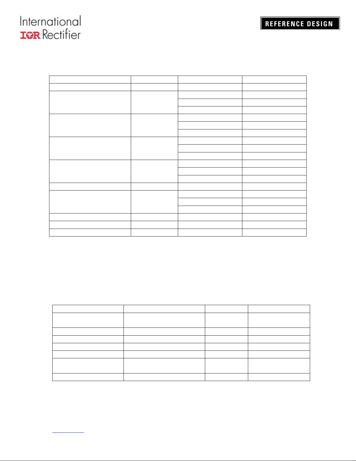
4. Electrical Characteristics
Parameter Units Dimming Level Value
Lamp Type 32W CFL
Maximum 31
Input Power [W]
Input Current [mArms]
Lamp Running Voltage [Vpp]
Lamp Running Current [mArms]
Start Frequency [kHz] 115
Run Frequency [kHz]
Preheat Time [s] 0.5
Input AC Voltage Range [VACrms] 60 - 180
Ballast turn-off voltage [VACrms] 60
TABLE 4.1: Ballast Parameters.
Intermediate 22
Minimum 15
Maximum 386
Intermediate 260
Minimum 175
Maximum 370
Intermediate 540
Minimum 630
Maximum 190
Intermediate 80
Minimum 27
Maximum 42
Intermediate 59
Minimum 60
5. Fault Protection Characteristics
Fault Protection Ballast Restart Operation
Brown-out Non-ZVS Increase
frequency
Upper filament broken Crest Factor Over Current Deactivates Lamp exchange
Lower filament broken Crest Factor Over Current Deactivates Lamp exchange
Lamp removed Crest Factor Over Current Deactivates Lamp inserted
Failure to ignite VVCOFLT+ Deactivates Lamp exchange
No lamp VLOSD- Does not
start
End of life Crest Factor Over Current Deactivates Lamp exchange
TABLE 5.1: Fault Protections Characteristics.
Line voltage
increase
Lamp inserted
www.irf.com
RD0803
- 9 -

6. Functional Description
The IRS2530D design utilizes a voltage doubler at the front end in all modes of operation
giving a fixed DC bus voltage approximately 300V. By correctly selecting value of the
snubber capacitor it is not difficult to achieve soft switching in all modes of operation.
The front end of the IRPLCFL8U ballast circuit shows the neutral line input (i.e. the one
that is always connected) connected to the center point of the DC bus storage capacitors
C3 and C4. Live inputs L1 and L2 are connected to two completely separate voltage
doubler diode pairs which are connected to the DC bus. These four diodes are all
contained within the bridge BR1 (This is shown as D1, D2, D3 and D4 in the schematic of
Fig 6). If live input L1 is connected to the line, a 60Hz sinusoidal AC voltage will be present
at the point where the anode of D1 joins the cathode of D3. This voltage will swing
between the 300V DC bus voltage and the 0V COM point of the circuit. If live input L1 is
not connected to the line this point will be floating with only residual voltage present. The
same applies with live input L2 at the point where the anode of D2 meets the cathode of
D4. These two points are fed via resistors R5 and R6 to the parallel combination of R7 and
C5, which are connected to 0V COM. The value of C5 is high enough to ensure that the
amount of ripple that is present at the junction of C5 and RDIM will be negligible so a DC
voltage will effectively appear there. This sets the reference voltage level for the dimming
feedback loop.
As a result this dimming control voltage will change depending on whether live input L1 is
connected only, live input L2 is connected only or both are connected, which depends on
the three way dimming rotary switch position. The values of R5 and R6 will be chosen so
that this voltage is substantially different if either live input L1 of live input L2 are
connected alone and these values are selected to set the desired low and mid light levels.
In this application R5 can be selected to give the correct reference voltage to provide 50%
light output as perceived by the human eye, which occurs at a point somewhat lower than
50% ballast power and R6 can be chosen for 75% which is at about 50% of the nominal
total ballast power at full light output.
The design problem overcome here is that the dimming control voltage obtained through
R5 and R6, where the values have been selected to provide minimum and medium light
outputs, is not sufficiently high to provide maximum light output when both live inputs are
connected. This being the case it was necessary to add the two pull up transistors Q1 and
Q2. When both inputs L1 and L2 are connected, i.e. when the rotary switch is in the fully
on position, the voltage at RDIM will be pulled high enough to ensure that the ballast
operates at maximum output since the transistors Q1 and Q2 will both be switched on in
this case.
Q1 and Q2 are small signal NPN devices, however they need to be rated to 300V VCEO
to prevent any conduction if either one is switched off. The zener diode DZ1 had been
added to ensure that Q1 and Q2 can fully switch off. This is because even when not
connected to the line some voltage appears at the bases of these devices. Since Q1 and
Q2 are configured as emitter followers the base voltage must exceed the breakdown
voltage of DZ1 (68V) in order to switch on, which can only occur when the corresponding
line input is connected through the rotary switch.
www.irf.com
RD0803
- 10 -

The closed loop regulation dimming ballast section, unlike in the IRPLCFL4 design, is
incorporated within the 8 pin package of the IRS2530D “simple dim” ballast controller
greatly simplifying the circuit design.
Since we are sensing the lamp arc current with a resistor it is necessary to use voltage
mode preheating to avoid detecting the sum of the current in the arc and the current in the
resonant output capacitor CRES. This has an additional advantage that during preheat
and prior to ignition of the lamp the arc current will always be zero and consequently the
feedback circuit will not influence the oscillator frequency until the lamp is running.
Consequently the preheat will occur in exactly the same way regardless of which of the
live inputs are connected, thus achieving optimum preheat and ignition under all
conditions.
A resistor parallel with CDC can be added if necessary to remove
the lamp that may occur at low dimming levels. However this has not been necessary in
this reference design.
R1 and R2 are fusible resistors that are optional and L1, L2, C1 and C2 are recommended
for EMI filtering but have no bearing on the functional operation of the ballast.
striations
(dark rings) in
Figure 6.1 shows the voltage at the DIM pin for all 3 dimming level.
Maximum Dim Level Intermediate Dim Level
Minimum Dim Level
www.irf.com
Figure 6.1: IRS2530D DIM pin voltages
RD0803
- 11 -

Figure 6.2 shows the voltage at the VCO pin, and the VS (half-bridge) voltage for all 3
dimming level.
Maximum Dim Level Intermediate Dim Level
Minimum Dim Level
Figure 6.2: IRS2530D VCO (red) and VS (yellow) pin voltages
www.irf.com
RD0803
- 12 -

Figure 6.3 shows the voltage across the lamp, and the current through the lamp for all 3
dimming level.
Maximum Dim Level Intermediate Dim Level
Minimum Dim Level
Figure 6.3: Lamp Voltage and Arc Current
www.irf.com
RD0803
- 13 -

Figure 6.4: Lamp Voltage and Arc Current during preheat and ignition
www.irf.com
RD0803
- 14 -

7. Fault Conditions
In case of fault conditions such as open filaments, failure to strike, or lamp removal, the
IRS2530D will go into Fault Mode. In this mode, the internal fault latch is set, HO is off, LO
is open circuit, and the IRS2530D consumes an ultra-low micro-power current. The
IRS2530D can be reset with a lamp exchange (as detected by the LO pin) or a recycling of
VCC below and back above the UVLO thresholds.
Failure to Strike
At initial turn-on of the ballast, the frequency will ramp down from f
resonance frequency. When the lamp fails to strike, the VCO voltage continues to
increase and the frequency continues to decrease until the VCO voltage exceeds
VVCOFLT+ (4.0V, typical), and the IRS2530D enters Fault Mode and shuts down
(Figure 7.1). It should be noted that in case of failure to strike, the system will operate in
capacitive side of resonance, but only for short period of time.
toward the
MAX
Figure 7.1: Lamp non-strike: CH1 is the VCO voltage, CH4 is the voltage across lamp
AC Mains Interrupt / Brown-Out Conditions
This protection relies on the non-ZVS circuit of IRS2530D, enabled in the Dim Mode.
During an AC mains interrupt or brown-out condition, the DC bus can decrease and
cause the system to operate too close to, or, on [the] capacitive side of resonance. The
result is non-ZVS switching that causes high peak currents to flow in the half-bridge
MOSFETs that can damage or destroy them.
To protect against this, the IRS2530D will detect non-ZVS by measuring the VS voltage
at each rising edge of LO. If the voltage is greater than VZVSTH (4.5V, typical), the IC
will reduce the voltage at VCO pin, and thus increase the frequency until ZVS is
reached again (Figure 7.2).
www.irf.com
RD0803
- 15 -

In case the DC bus decreases too far and the lamp extinguishes, the VCC voltage will
go below VCCUV- and the ignition/preheat ramp will be reset to re-ignite the lamp
reliably.
Figure 7.2: Brown-out conditions: CH1 is the VCO voltage, CH2 is the VS voltage
Lamp Removal
When the lamp is removed, the IRS2530D uses the Crest Factor Over-current
Protection to enter the Fault mode and shut down. During lamp removal, the output
stage will transition to a series-LC configuration, and the frequency will move towards
resonance until the inductor saturates. The IRS2530D uses the VS-sensing circuitry
and the RDSon of the low-side half-bridge MOSFET to measure the MOSFET current
for detecting an over-current fault. Should the peak current exceed the average current
by a factor of 5.5 (CF>5.5) during the on-time of LO, the IRS2530D will enter Fault
Mode, where the half-bridge is off. Performing crest factor measurement provides a
relative current measurement that cancels temperature and/or tolerance variations of
the RDSon of the low-side half-bridge MOSFET.
Figure 7.3 shows the voltage across the lamp and the VS voltage when the lower
filament of the lamp is removed. Figure 7.4 shows these voltages when the upper
filament of the lamp is removed. In both cases, the IRS2530D will enter the Fault Mode
and shut down after detecting that the crest factor exceeds 5 during the on-time of LO.
Figure 7.5 shows the VS pin, inductor current, and voltage across lamp when the
inductor saturates and the ballast shuts down.
www.irf.com
RD0803
- 16 -

Figure 7.3: Lower filament removed: CH2 is the VS voltage, CH4 is the voltage across the lamp
Figure 7.4: Upper filament removed: CH2 is the VS voltage, CH4 is the voltage across the lamp
www.irf.com
RD0803
- 17 -

Figure 7.5: Inductor saturation: CH1 is the LO voltage, CH2 is the VS voltage, CH3 is the current
through the resonant inductor, and CH4 is the voltage across the lamp
Figure 7.6 shows the VS voltage and the voltage across the lamp when the IC undergoes
reset with a lamp exchange. When the lamp is removed, crest factor protection is
triggered, and the IC enters the Fault mode and shuts down. Since the lamp is removed,
LO pins is pulled above VLOSD+, and the IC goes to UVLO mode. When the lamp is reinserted, the IC goes back to the Preheat / Ignition mode, and the half-bridge starts to
oscillate again.
Figure 7.6: Lamp exchange: CH1 is the LO voltage, CH2 is the VS voltage, and CH4 is the voltage across
the lamp
www.irf.com
RD0803
- 18 -

8. Ballast Design
Layout Guidelines
Proper care should be taken when laying out a PCB board to minimize noise effects
due to high-frequency switching and to ensure proper functionality of the IRS2530D.
1. There should be a star point for all of the 0V returns, particularly IC1 pin 2,
CVCC, CDIM, CVCO, CCPH, R7 and C5, which is then connected to the source
of the lower half-bridge MOSFET(ML) via a single trace which is as short as
possible. This avoids potential ground loop problems.
2. The VCC decoupling capacitor (CVCC2) should be placed as close to the
IRS2530D VCC (pin 1) and COM (pin 2) as possible with the shortest possible
traces.
3. Double filter at VCC (RVCC1, CVCC1, RVCC2, and CVCC2) should be utilized
to filter high current spikes that can cause large voltage spikes to occur on VCC.
4. All IC programming and filter components should be placed as close as possible
between their respective pins and COM (CVCO, RVCO, CCPH, CDIM, CFB,
RFB).
5. Keep RCS, RFB and CFB as far away as possible from the VS node to prevent
high-frequency, high-voltage switching noise from interfering with dimming
feedback signal.
6. The high-side gate-drive ground (VS) should be connected to half-bridge midpoint at one connection only.
7. The anode of charge pump diode DCP1 should be connected to the power
ground not the signal ground.
8. Use gate resistors (RLO, RHO) between all gate driver outputs and the gate of
their respective power MOSFETs.
IRS2530D
SIGNAL GROUND
STAR POINT AT IC COM
IC PROGRAMMING AND
FILTER COMPONENTS
CFB, RFB, AND RCS ARE AS FAR
AWAY AS POSSIBLE FROM VS NODE
Figure 8.1: Critical traces on the bottom side of the PCB
www.irf.com
RD0803
VS NODE
SINGLE TRACE JOINING
VS-PIN AND HALF-BRIDGE
MID-POINT
VCC DECOUPLING
CAPACITOR
- 19 -

ANODE OF CHARGE PUMP
DIODE DCP1 IS CONNECTED TO
POWER GROUND
Figure 8.2: Critical traces on the top side of the PCB
SINGLE TRACE JOINING STAR
POINT AND THE SOURCE OF
LOWER HALF-BRIDGE MOSFET
Components Selection
The output inductor and capacitor values should be chosen to allow the ballast to run at
maximum brightness around 40-45kHz. This will minimize losses in the inductor. For
this example the
IR Ballast Designer
software * has been used to select the required
preheat, ignition and run frequencies for a 32W spiral CFL lamp giving an LRES of
2.2mH and CRES of 4.7nF.
Output Inductor Design
The output inductor LRES should be designed to allow a high peak ignition current
without saturating. This is important as the IRS2530D shutdown will be triggered if the
inductor saturates. The ignition current depends on the type of lamp being used and
must be kept to a minimum by ensuring the preheat is sufficient. To minimize losses in
the inductor multi-stranded wire should be used in combination with Ferrite cores of
adequate quality. The best approach to design is to wind as many turns as possible of
multi-stranded wire and have the largest gap possible to achieve the correct
inductance. This will produce the highest available peak current before saturating the
inductor. It is important to be aware that when the cores are hot the saturation point and
hence the peak current for the inductor will be lower therefore a poorly designed
inductor may result in the ballast shutting down during an attempted hot re-strike.
The inductor design process can be greatly simplified by using the
software produced by I.R. For this application and lamp size it is recommended to fix
the core size to EF20.
www.irf.com
RD0803
Ballast Designer
- 20 -

Ballast Designer
Lamp Preheating
The lamp must be sufficiently preheated before ignition. The correct preheat current
can be determined from published data or from International Rectifiers
software.
The preheat time can be set by adjusting the value of CPH. As a general rule the lamp
filament should glow red before ignition. If preheat is insufficient the ballast is likely to
shutdown during ignition because the output inductor will be unable to operate at the
high current required. The number of turns in the auxiliary cathode windings of the
output inductor LRES should be chosen to provide sufficient preheat. In designs for
ballasts with integral lamps the shutdown pin can be grounded so that the inductor may
saturate without shutting down the circuit.
The lamp filament (Cathode) resistance over the range of dimming levels should be
between 3 and 5.5 times the resistance when cold. A simple method for determining
the hot resistance is to first connect one cathode to a DC power supply via an ammeter
and slowly increase the voltage from zero, noting the current at 1V intervals. This
should be done until the cathode can be seen to be glowing red. When this occurs the
voltage should not be increased further in order to prevent possible cathode damage.
The resistance can then be calculated for each voltage and hence the acceptable
voltage range can be found to comply with the 3 to 5.5 times cold resistance, which can
be easily measured with a digital multi-meter (DMM).
Then when the ballast is being run a true RMS digital voltmeter can be connected
across one cathode and the voltage can be observed at maximum and minimum
brightness. The cathode voltage increases as the ballast is dimmed. The values of
CH1 and CH2 will control how much it increases by, reducing the capacitance will
reduce the amount by which the voltage rises. The values should be chosen to prevent
the voltage exceeding the upper limit at minimum output.
It is important to consider that using additional windings on the inductor to provide
cathode heating means that power is now being transferred through the core and
consequently the core losses will increase and hence the core operating temperature.
The core will reach its highest operating temperature when the ballast is running at
minimum brightness.
www.irf.com
RD0803
- 21 -

9. Bill of Materials
Item # Qty Manufacturer Part Number Description Reference
1 1 International Rectifier IRS2530D Ballast Controller IC1
2 2 International Rectifier IRF730 MOSFET MH,ML
3 2 Fairchild MMBTA42 Transistor 300V, SOT-23 Q1,Q2
4 1 Diodes Inc ZMM5266B-7 Zener Diode 68V DZ1
5 1 Diodes Inc ZMM5230B-7 Zener Diode, 4V7 DZ2
6 2 Diodes Inc LL4148-13 Small Signal Diode SMD DCP1, DCP2
7 1 Fairchild DF10S Bridge SMD BR1
8 2 Renco RL-5480-3-2700 Filter Inductor L1,L2
9 1 Vogt IL 070 503 11 02 Inductor 2.2mH EF20 LRES
10 2 Panasonic-ECG ECQ-E2104KB Capacitor 100nF, 250V C1,2
11 2 Panasonic-ECG ECA-2EHG330 Capacitor, 33uF 250V 105C
Electrolytic
12 1 Panasonic-ECG ECJ-3YX1C106K Capacitor 10u, 16V, 1206 C5
13 2 Panasonic-ECG ECJ-3YB1C225K Capacitor 2u2, 16V, 1206 CVCC1, CVCC2
14 1 Panasonic-ECG ECJ-3YC2D102J Capacitor 1nF, 200V, 1206 CDIM
15 1 Panasonic-ECG ECJ-3VB1C334K Capacitor 0.33uF, 16V, 1206 CCPH
16 1 Panasonic-ECG ECJ-3VC2A222J Capacitor 2n2, 100V, 1206 CVCO
17 2 Panasonic-ECG ECJ-3VB1H104K Capacitor 100nF, 50V, 1206 CFB, CBS
18 2 Panasonic-ECG ECJ-3YB1H224K Capacitor 220nF, 50V, 1206 CH1, CH2
19 1 Panasonic-ECG ECK-A3A102KBP Capacitor 1nF, 1kV, Ceramic CSNUB
20 1 Wima MKS2 Series Capacitor 47nF, 400V CDC
21 1 Wima MKP10 Series Capacitor 4.7nF, 1600V,
15mm, Pulse
22 2 Yageo CFR-50JB-5R6 5.6R 1/2W Axial R1, R2
23 4 Panasonic-ECG ERJ-8GEYJ105V Resistor, 1M, 0.25W, 1206 R3, R4, R6,
24 1 Panasonic-ECG ERJ-8GEYJ334V Resistor, 330K, 0.25W, 1206 R5
25 1 Panasonic-ECJ ERJ-8GEYJ202V Resistor, 2K, 0.25W 1206 R7
26 1 Panasonic-ECJ ERJ-8GEYJ154V Resistor, 150K, 0.25W, 1206 RPU
27 2 Panasonic-ECJ ERJ-8GEYJ100V Resistor, 10R, 0.25W, 1206 RVCC1, RVCC2
28 1 Panasonic-ECJ ERJ-8GEYJ103V Resistor, 10K, 0.25W, 1206 RDIM
29 1 Panasonic-ECJ ERJ-8GEYJ152V Resistor, 1K5, 0.25W, 1206 RVCO
30 1 Panasonic-ECJ ERJ-8GEYJ102V Resistor, 1K, 0.25W, 1206 RFB
31 2 Panasonic-ECJ ERJ-8GEYJ220V Resistor, 22R, 0.25W, 1206 RHO, RLO
32 1 Panasonic-ECJ ERJ-8GEYJ474V Resistor, 470K, 0.25W, 1206 RLMP1
33 2 Panasonic-ECJ ERJ-8GEYJ274V Resistor, 270K, 0.25W, 1206 RS1, RS2
34 1 Phoenix Passive
Components
TABLE 9.1: IRPLCFL8U Bill of Materials.
5073NW15R00J12
AFX
Resistor, 15R, 1W, Axial RCS
C3,4
CRES
RLMP2
www.irf.com
RD0803
- 22 -

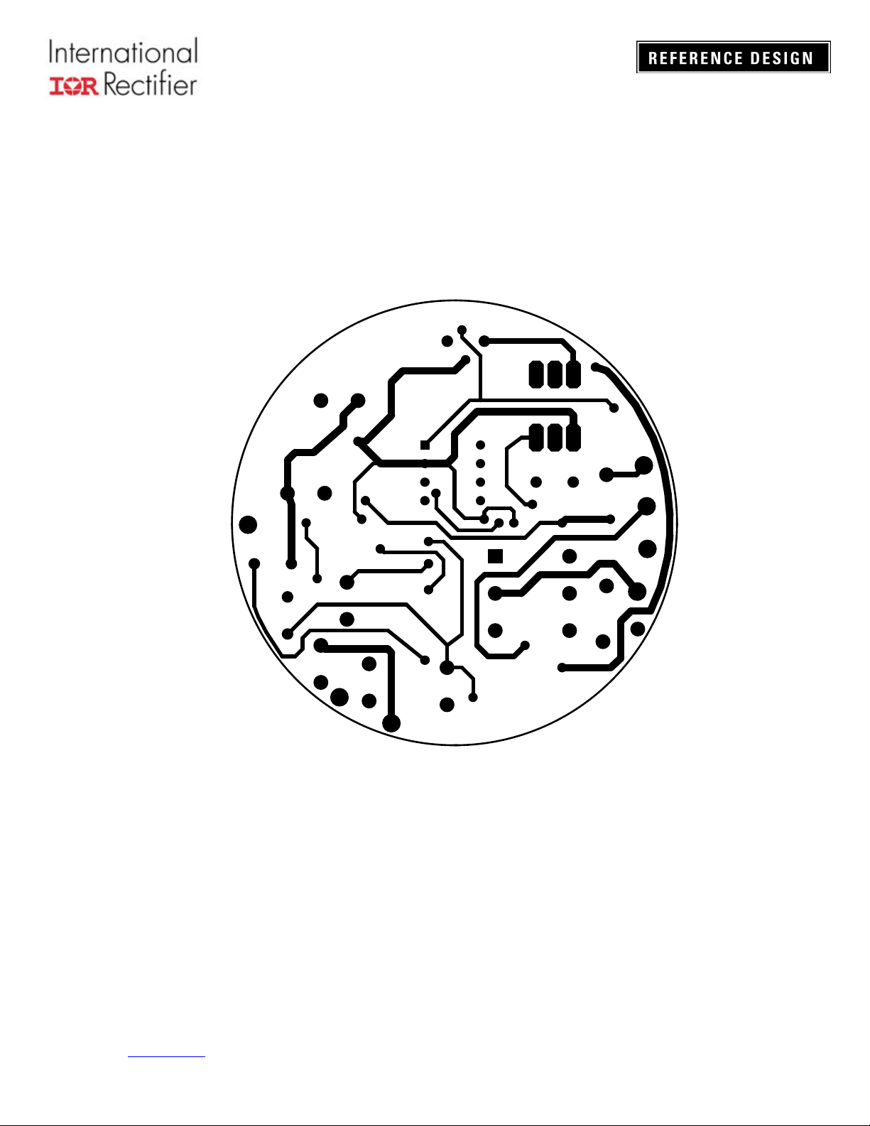
10. IRPLCFL8U PCB Layout
Top Assembly
www.irf.com
RD0803
- 23 -
Top Copper
www.irf.com
RD0803
- 24 -

Bottom Assembly
www.irf.com
RD0803
- 25 -

Bottom Copper
www.irf.com
RD0803
- 26 -

11. Inductor Specifications
Vogt # IL 070 503 11 02
BI Technologies # HM00-07544
INDUCTOR SPECIFICATION
CORE SIZE
GAP LENGTH
CORE MATERIAL
NOMINAL INDUCTANCE
TEST TEMPERATURE C
WINDING START PIN
MAIN
CATHODE
CATHODE
PHYSICAL LAYOUT
( Vertical 6- Pin Bobbin)
1
2 5
3 4
E20/10/ 6 (EF20)
1.0
mm
Philips 3C85 , Siemens N27 or equivalent
2.3
mH
100
FINISH PIN TURNS WIRE DIAMETER (mm
6
240*
5.5
5.5
10/ 38 Multistranded
26 awg insulated
26 awg insulated
0.4"
6
1
)
Pin View
5
2
0.4"
34
TEST
MAIN WINDING INDUCTANCE
TEST TEMPERATURE C
100
MIN 2.1
mH
MAX 2.4
* Adjust turns for specified Inductance
mH
www.irf.com
RD0803
- 27 -
 Loading...