

查询IRFD420供应商
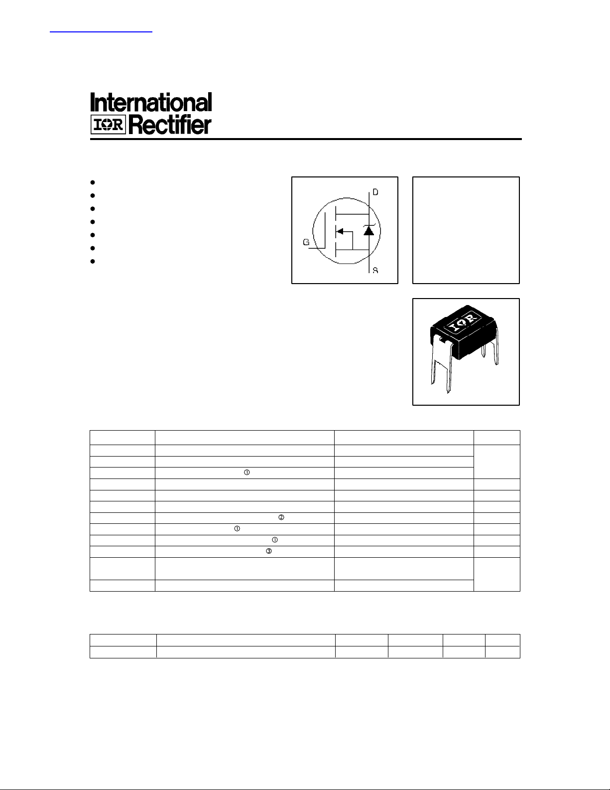
HEXFET® Power MOSFET
Dynamic dv/dt Rating
Repetitive Avalanche Rated
For Automatic Insertion
End Stackable
Fast Switching
Ease of paralleling
Simple Drive Requirements
Description
Third Generation HEXFETs from International Rectifier provide the designer
with the best combination of fast switching, ruggedized device design, low onresistance and cost-effectiveness.
PD -9.1227
IRFD420
V
= 500V
DSS
R
ID = 0.37A
DS(on)
= 3.0Ω
The 4-pin DIP package is a low-cost machine-insertable case style which can be
stacked in multiple combinations on standard 0.1 inch pin centers. The dual drain
serves as a thermal link to the mounting surface for power dissipation levels up to
1 watt.
HD-1
Absolute Maximum Ratings
Parameter Max. Units
ID @ TC = 25°C Continuous Drain Current, VGS @ 10 V 0.37
ID @ TC = 100°C Continuous Drain Current, VGS @ 10 V 0.23 A
I
DM
PD @TC = 25°C Power Dissipation 1.0 W
V
GS
E
AS
I
AR
E
AR
dv/dt Peak Diode Recovery dv/dt 3.5 V/ns
T
J
T
STG
Pulsed Drain Current 3.0
Linear Derating Factor 0.0083 W/°C
Gate-to-Source Voltage ±20 V
Single Pulse Avalanche Energy 51 mJ
Avalanche Current 0.37 A
Repetitive Avalanche Energy 0.10 mJ
Operating Junction and -55 to + 150
Storage Temperature Range °C
Soldering Temperature, for 10 seconds 300 (1.6mm from case)
Thermal Resistance
A
Parameter Min. Typ. Max. Units
R
θJA
Junction-to-Ambient — — 120 °C/W
Revision 0
IRFD420
Electrical Characteristics @ TJ = 25°C (unless otherwise specified)
Parameter Min. Typ. Max. Units Conditions
V
(BR)DSS
∆V
(BR)DSS
R
DS(on)
V
GS(th)
g
fs
I
DSS
I
GSS
Q
g
Q
gs
Q
gd
t
d(on)
t
r
t
d(off)
t
f
L
D
L
S
C
iss
C
oss
C
rss
Drain-to-Source Breakdown Voltage 500 — — V VGS = 0V, ID = 250µA
/∆T
Breakdown Voltage Temp. Coefficient — 0.59 — V/°C Reference to 25°C, ID = 1mA
J
Static Drain-to-Source On-Resistance — — 3.0 Ω VGS = 10.0V, ID = 0.22A
Gate Threshold Voltage 2.0 — 4.0 V VDS = VGS, ID = 250µA
Forward Transconductance 1.5 — — S VDS = 50V, ID = 1.3A
Drain-to-Source Leakage Current — — 25 VDS = 500V, VGS = 0V
— — 250 VDS = 400V, VGS = 0V, TJ = 125°C
Gate-to-Source Forward Leakage — — 100 VGS = 20V
Gate-to-Source Reverse Leakage — — -100 VGS = -20V
µA
nA
Total Gate Charge — — 24 ID = 2.1A
Gate-to-Source Charge — — 3.3 nC VDS = 400V
Gate-to-Drain ("Miller") Charge — — 13 VGS = 10V
Turn-On Delay Time — 8.0 — VDD = 250V
Rise Time — 8.6 — ID = 2.1A
Turn-Off Delay Time — 33 — RG = 18Ω
ns
Fall Time — 16 — RD = 120Ω
Internal Drain Inductance — 4.0 — Between lead,
6mm (0.25in.)
Internal Source Inductance — 6.0 — from package
nH
and center of
die contact
Input Capacitance — 360 — VGS = 0V
Output Capacitance — 92 — pF VDS = 25V
Reverse Transfer Capacitance — 37 — ƒ = 1.0MHz
Source-Drain Ratings and Characteristics
Parameter Min. Typ. Max. Units Conditions
I
S
I
SM
V
SD
t
rr
Q
rr
t
on
Notes:
Repetitive rating; pulse width limited by
max. junction temperature.
V
DD
RG = 25Ω, I
Continuous Source Current MOSFET symbol
(Body Diode) showing the
Pulsed Source Current integral reverse
(Body Diode) p-n junction diode.
— — 0.37
— — 5.0
Diode Forward Voltage — — 1.6 V TJ = 25°C, IS = 0.37A, VGS = 0V
Reverse Recovery Time — 260 520 ns TJ = 25°C, IF = 2.1A
Reverse RecoveryCharge — 0.70 1.4 µC di/dt = 100A/µs
Forward Turn-On Time
Intrinsic turn-on time is negligible (turn-on is dominated by LS+LD)
I
≤ 4.4A, di/dt ≤ 90A/µs, V
SD
TJ ≤ 150°C
= 50V, starting TJ = 25°C, L = 40mH
= 1.5A.
AS
Pulse width ≤ 300µs; duty cycle ≤ 2%.
A
DD
≤ V
(BR)DSS
,
IRFD420
R
DS(on)
, Drain-to-Source On Resistance
(Normalized)
I
D
, Drain Current (Amps)
I
D
, Drain Current (Amps)
I
D
, Drain Current (Amps)
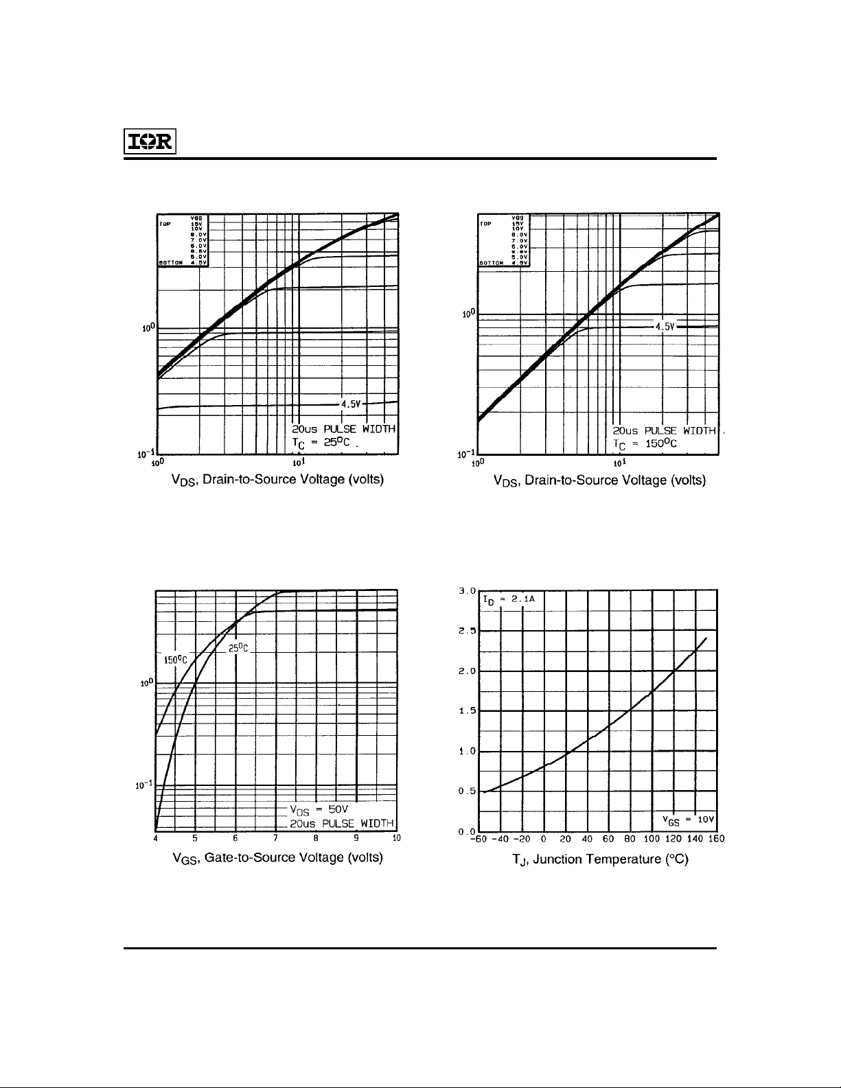
Fig 1. Typical Output Characteristics,
TC = 25oC
Fig 2. Typical Output Characteristics,
TC = 150oC
Fig 3. Typical Transfer Characteristics Fig 4. Normalized On-Resistance
Vs. Temperature

IRFD420
Capacitance (pF)
V
GS
, Gate-to-Source Voltage (volts)
I
SD
, Reverse Drain Current (Amps)
I
D
, Drain Current (Amps)
Fig 5. Typical Capacitance Vs.
Drain-to-Source Voltage
Fig 7. Typical Source-Drain Diode
Forward Voltage
Fig 6. Typical Gate Charge Vs.
Gate-to-Source Voltage
Fig 8. Maximum Safe Operating Area

IRFD420
I
D
, Drain Current (Amps)
Fig 10a. Switching Time Test Circuit
Fig 9. Maximum Drain Current Vs.
Case Temperature
Fig 11. Maximum Effective Transient Thermal Impedance, Junction-to-Case
Fig 10b. Switching Time Waveforms

IRFD420
Fig 12a. Unclamped Inductive Test Circuit
Fig 12c. Maximum Avalanche Energy
Vs. Drain Current
Fig 12b. Unclamped Inductive Waveforms
Fig 13a. Basic Gate Charge Waveform
Fig 13b. Gate Charge Test Circuit

dv/dt Test Circuit
IRFD420
Peak Diode Recovery Test Circuit

IRFD420
Package Outline
WORLD HEADQUARTERS: 233 Kansas St., El Segundo, California 90245, Tel: (310) 322 3331
IR CANADA: 7321 Victoria Park Ave., Suite 201, Markham, Ontario L3R 3L1, Tel: (905) 475 1897 IR GERMANY:
Saalburgstrasse 157, 61350 Bad Homburg Tel: 6172 37066 IR ITALY: Via Liguria 49, 10071 Borgaro, Torino Tel: (39)
1145 10111 IR FAR EAST: K&H Bldg., 2F, 3-30-4 Nishi-Ikeburo 3-Chome, Toshima-Ki, Tokyo 171 Tel: (03)3983 0641
IR SOUTHEAST ASIA: 315 Outram Road, #10-02 Tan Boon Liat Building, 0316 Tel: 65 221 8371
EUROPEAN HEADQUARTERS: Hurst Green, Oxted, Surrey RH8 9BB, UK Tel: (44) 0883 713215
Data and specifications subject to change without notice.
 Loading...