International Rrectifier IRF2805S User Manual

查询IRF2805L供应商
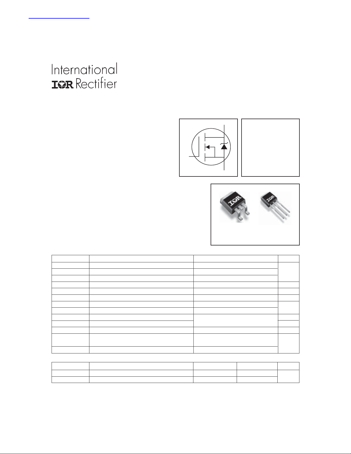
Typical Applications
● Climate Control
● ABS
● Electronic Braking
● Windshield Wipers
Features
● Advanced Process Technology
● Ultra Low On-Resistance
● 175°C Operating Temperature
● Fast Switching
● Repetitive Avalanche Allowed up to Tjmax
Description
Specifically designed for Automotive applications, this
HEXFET® Power MOSFET utilizes the latest processing
techniques to achieve extremely low on-resistance per
silicon area. Additional features of this product are a 175°C
junction operating temperature, fast switching speed and
improved repetitive avalanche rating . These features combine to make this design an extremely efficient and reliable
device for use in Automotive applications and a wide variety
of other applications.
Absolute Maximum Ratings
ID @ TC = 25°C Continuous Drain Current, VGS @ 10V 135V
ID @ TC = 100°C Continuous Drain Current, VGS @ 10V 96V A
I
DM
PD @TC = 25°C Power Dissipation 200 W
V
GS
E
AS
E
(6 sigma) Single Pulse Avalanche Energy Tested ValueX 1220
AS
I
AR
E
AR
dv/dt Peak Diode Recovery dv/dt S 2.0 V/ns
T
J
T
STG
Thermal Resistance
R
θJC
R
θJA
HEXFET(R) is a registered trademark of International Rectifier.
www.irf.com 1
PD - 94428
IRF2805S
AUTOMOTIVE MOSFET
HEXFET® Power MOSFET
D
G
S
D2Pak
IRF2805S
Parameter Max. Units
Pulsed Drain Current Q 700
Linear Derating Factor 1.3 W/°C
Gate-to-Source Voltage ± 20 V
Single Pulse Avalanche EnergyR 380 mJ
Avalanche CurrentQ See Fig.12a, 12b, 15, 16 A
Repetitive Avalanche EnergyW mJ
Operating Junction and -55 to + 175
Storage Temperature Range
Soldering Temperature, for 10 seconds 300 (1.6mm from case )
Parameter Typ. Max. Units
Junction-to-Case ––– 0.75
Junction-to-Ambient(PCB Mounted, steady state)** ––– 40
IRF2805L
V
= 55V
DSS
R
= 4.7mΩ
DS(on)
ID = 135AV
TO-262
IRF2805L
°C
°C/W
06/10/02

IRF2805S/IRF2805L
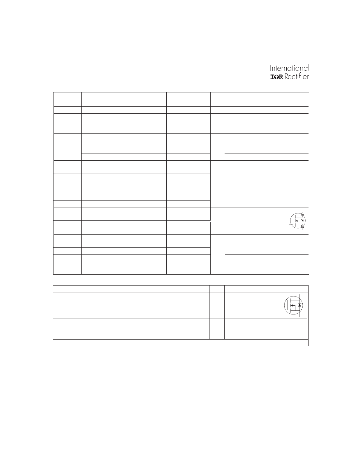
Electrical Characteristics @ TJ = 25°C (unless otherwise specified)
Parameter Min. Typ. Max. Units Conditions
V
(BR)DSS
∆V
(BR)DSS
R
DS(on)
V
GS(th)
g
fs
I
DSS
I
GSS
Q
g
Q
gs
Q
gd
t
d(on)
t
r
t
d(off)
t
f
L
D
L
S
C
iss
C
oss
C
rss
C
oss
C
oss
C
eff. Effective Output Capacitance U ––– 1600 ––– VGS = 0V, VDS = 0V to 44V
oss
Source-Drain Ratings and Characteristics
I
S
I
SM
V
SD
t
rr
Q
rr
t
on
Notes:
Q Repetitive rating; pulse width limited by
max. junction temperature. (See fig. 11).
R Starting T
RG = 25Ω, I
S I
SD
TJ ≤ 175°C
T Pulse width ≤ 400µs; duty cycle ≤ 2%.
2 www.irf.com
Drain-to-Source Breakdown Voltage 55 ––– ––– V VGS = 0V, ID = 250µA
/∆T
Breakdown Voltage Temp. Coefficient ––– 0.06 ––– V/°C Reference to 25°C, ID = 1mA
J
Static Drain-to-Source On-Resistance ––– 3.9 4.7 mΩ VGS = 10V, ID = 104A T
Gate Threshold Voltage 2.0 ––– 4.0 V VDS = 10V, ID = 250µA
Forward Transconductance 91 ––– ––– S VDS = 25V, ID = 104A
Drain-to-Source Leakage Current
––– ––– 20
––– ––– 250 VDS = 44V, VGS = 0V, TJ = 150°C
Gate-to-Source Forward Leakage ––– ––– 200 VGS = 20V
Gate-to-Source Reverse Leakage ––– ––– -200
VDS = 55V, VGS = 0V
µA
nA
VGS = -20V
Total Gate Charge ––– 150 230 ID = 104A
Gate-to-Source Charge ––– 38 57 nC VDS = 44V
Gate-to-Drain ("Miller") Charge ––– 52 78 VGS = 10VT
Turn-On Delay Time ––– 14 ––– VDD = 28V
Rise Time ––– 120 ––– ID = 104A
Turn-Off Delay Time ––– 68 ––– RG = 2.5Ω
ns
Fall Time ––– 110 ––– VGS = 10V T
4.5
Internal Drain Inductance
Internal Source Inductance ––– –––
––– –––
7.5
Between lead,
6mm (0.25in.)
nH
from package
and center of die contact
Input Capacitance ––– 5110 ––– VGS = 0V
Output Capacitance ––– 1190 ––– pF VDS = 25V
Reverse Transfer Capacitance ––– 210 ––– ƒ = 1.0MHz, See Fig. 5
Output Capacitance ––– 6470 ––– VGS = 0V, VDS = 1.0V, ƒ = 1.0MHz
Output Capacitance ––– 860 ––– VGS = 0V, VDS = 44V, ƒ = 1.0MHz
Parameter Min. Typ. Max. Units Conditions
Continuous Source Current MOSFET symbol
(Body Diode)
Pulsed Source Current integral reverse
(Body Diode) Q
––– –––
––– –––
175V
700
showing the
A
p-n junction diode.
Diode Forward Voltage ––– ––– 1.3 V TJ = 25°C, IS = 104A, VGS = 0VT
Reverse Recovery Time ––– 80 120 ns TJ = 25°C, IF = 104A
Reverse Recovery Charge ––– 290 430 nC di/dt = 100A/µs
T
Forward Turn-On Time Intrinsic turn-on time is negligible (turn-on is dominated by LS+LD)
U C
eff. is a fixed capacitance that gives the same charging time
oss
= 25°C, L = 0.08mH
J
= 104A. (See Figure 12).
AS
≤ 104A, di/dt ≤ 240A/µs, V
DD
≤ V
(BR)DSS
as C
V Calculated continuous current based on maximum allowable
junction temperature. Package limitation current is 75A.
W Limited by T
,
avalanche performance.
oss
while V
is rising from 0 to 80% V
DS
, see Fig.12a, 12b, 15, 16 for typical repetitive
Jmax
DSS
.
X This value determined from sample failure population. 100%
tested to this value in production.
G
G
D
S
D
S

IRF2805S/IRF2805L
1000
100
VGS
TOP 15V
10V
8.0V
7.0V
6.0V
5.5V
5.0V
BOTTOM 4.5V
4.5V
10
, Drain-to-Source Current (A)
D
I
20µs PULSE WIDTH
1
0.1 1 10 100
Tj = 25°C
VDS, Drain-to-Source Voltage (V)
1000
TJ = 25°C
A)
TJ = 175°C
1000
100
, Drain-to-Source Current (A)
D
I
VGS
TOP 15V
10V
8.0V
7.0V
6.0V
5.5V
5.0V
BOTTOM 4.5V
4.5V
20µs PULSE WIDTH
10
0.1 1 10 100
Tj = 175°C
VDS, Drain-to-Source Voltage (V)
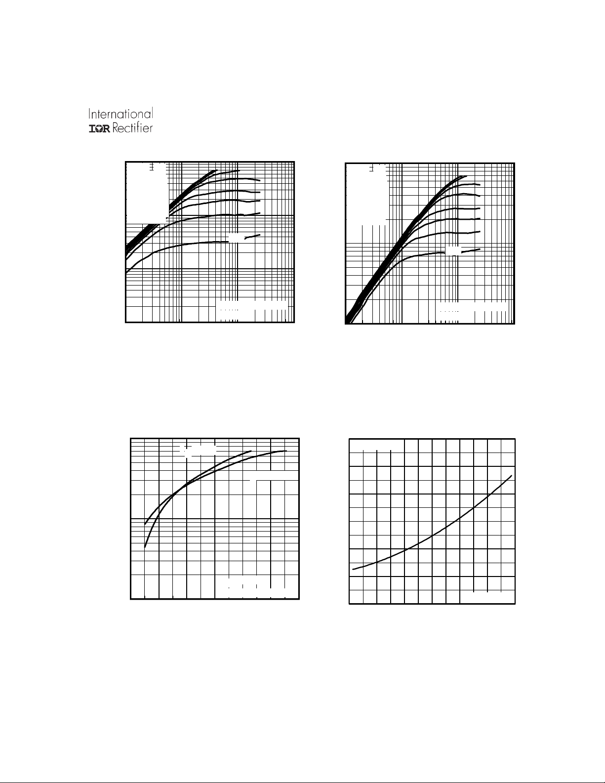
Fig 2. Typical Output CharacteristicsFig 1. Typical Output Characteristics
3.0
175A
I =
D
2.5
2.0
100
, Drai n-to-Sour c e Current
D
I
10
4.0 5.0 6.0 7.0 8.0 9.0 10.0
V
= 25V
DS
20µs PULSE W IDTH
VGS, Gate-to-Source Voltage (V)
Fig 3. Typical Transfer Characteristics
1.5
(Normalized)
1.0
0.5
DS(on)
R , Drain-to-Source On Resistance
0.0
-60 -40 -20 0 20 40 60 80 100 120 140 160 180
T , Junction Temperature ( C)
J
Fig 4. Normalized On-Resistance
V =
10V
GS
°
Vs. Temperature
www.irf.com 3

IRF2805S/IRF2805L
10000
8000
6000
4000
C, Capacitance (pF)
2000
0
1 10 100
V
= 0V, f = 1 MHZ
GS
C
= C
iss
SHORTED
C
= C
rss
C
= C
oss
VDS, Dr ain-to-Sour ce Voltage (V)
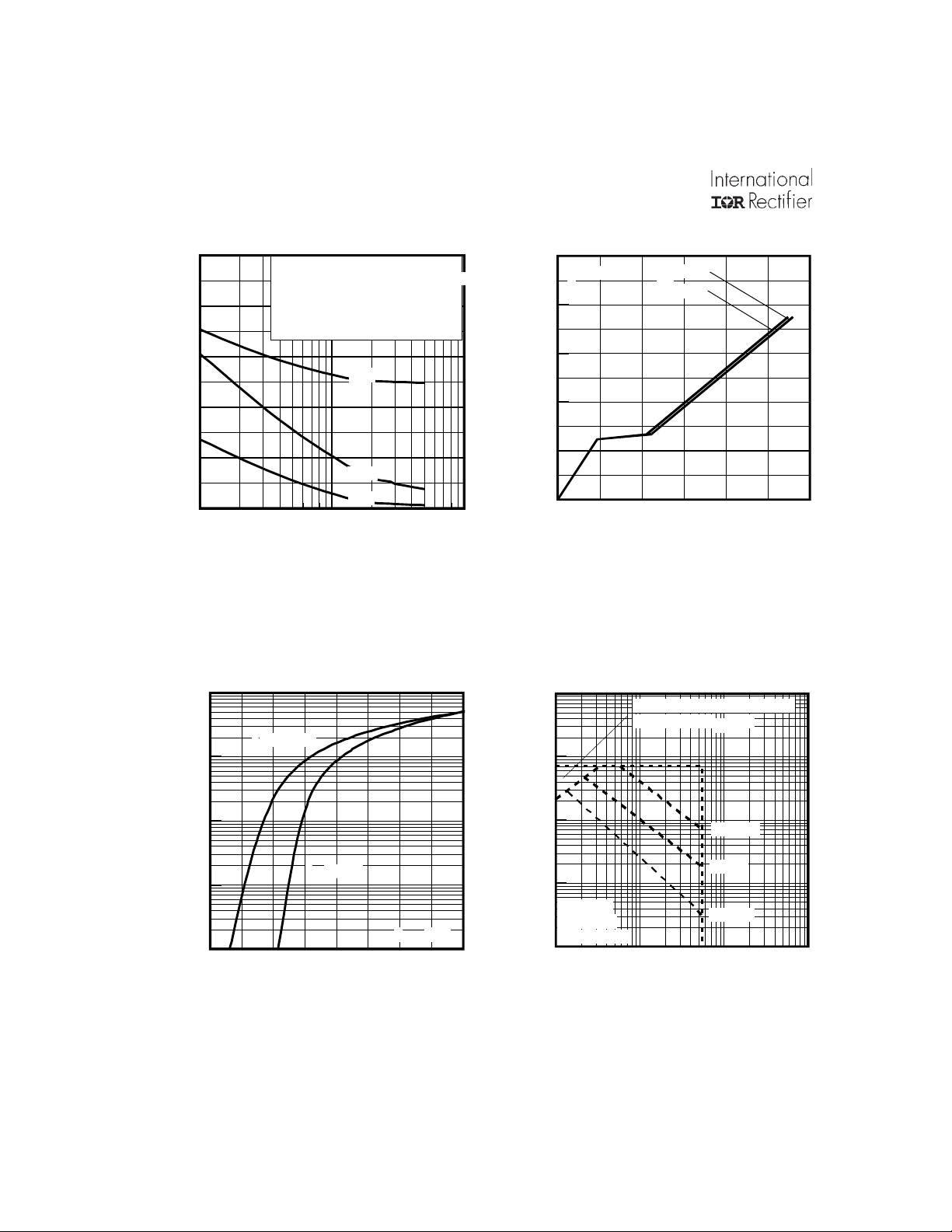
Fig 5. Typical Capacitance Vs.
Drain-to-Source Voltage
1000.0
TJ = 175°C
100.0
gd
ds
gs
+ C
Ciss
Cos s
Crss
gd
+ Cgd, C
ds
20
ID= 104A
16
12
8
, Gate-to-So urce Voltage (V)
4
GS
V
0
0 40 80 120 160 200 240
Q
VDS= 44V
VDS= 28V
Total Gate Charge (nC)
G
Fig 6. Typical Gate Charge Vs.
Gate-to-Source Voltage
10000
1000
OPERATION IN THIS AREA
LIMITED BY RDS(on)
, Drain-to-Source Current (A)
D
I
100
10
Tc = 25°C
Tj = 175°C
Singl e P ulse
1
1 10 100 1000
V
, Drain-toSource Voltage (V)
DS
100µsec
1msec
10msec
Fig 8. Maximum Safe Operating Area
10.0
, Reverse Drain Current (A)
I
1.0
SD
0.1
0.2 0.4 0.6 0.8 1. 0 1.2 1.4 1. 6 1.8
VSD, Source-toDrain Voltage (V)
TJ = 25°C
Fig 7. Typical Source-Drain Diode
V
GS
= 0V
Forward Voltage
4 www.irf.com
 Loading...