

A
查询IRF1902供应商
l Ultra Low On-Resistance
l N-Channel MOSFET
l Surface Mount
l Available in Tape & Reel
PD - 94282A
IRF1902
HEXFET® Power MOSFET
V
DSS
R
DS(on)
max (m
20V 85@VGS = 4.5V 4.0A
170@VGS = 2.7V 3.2A
Ω)Ω)
Ω) I
Ω)Ω)
D
Description
These N-Channel HEXFET
International Rectifier utilize advanced processing
techniques to achieve the extremely low on-resistance
per silicon area. This benefit provides the designer
with an extremely efficient device for use in battery
power MOSFETs from
1
S
2
S
3
S
4
A
8
D
7
D
6
D
5
DG
and load management applications..
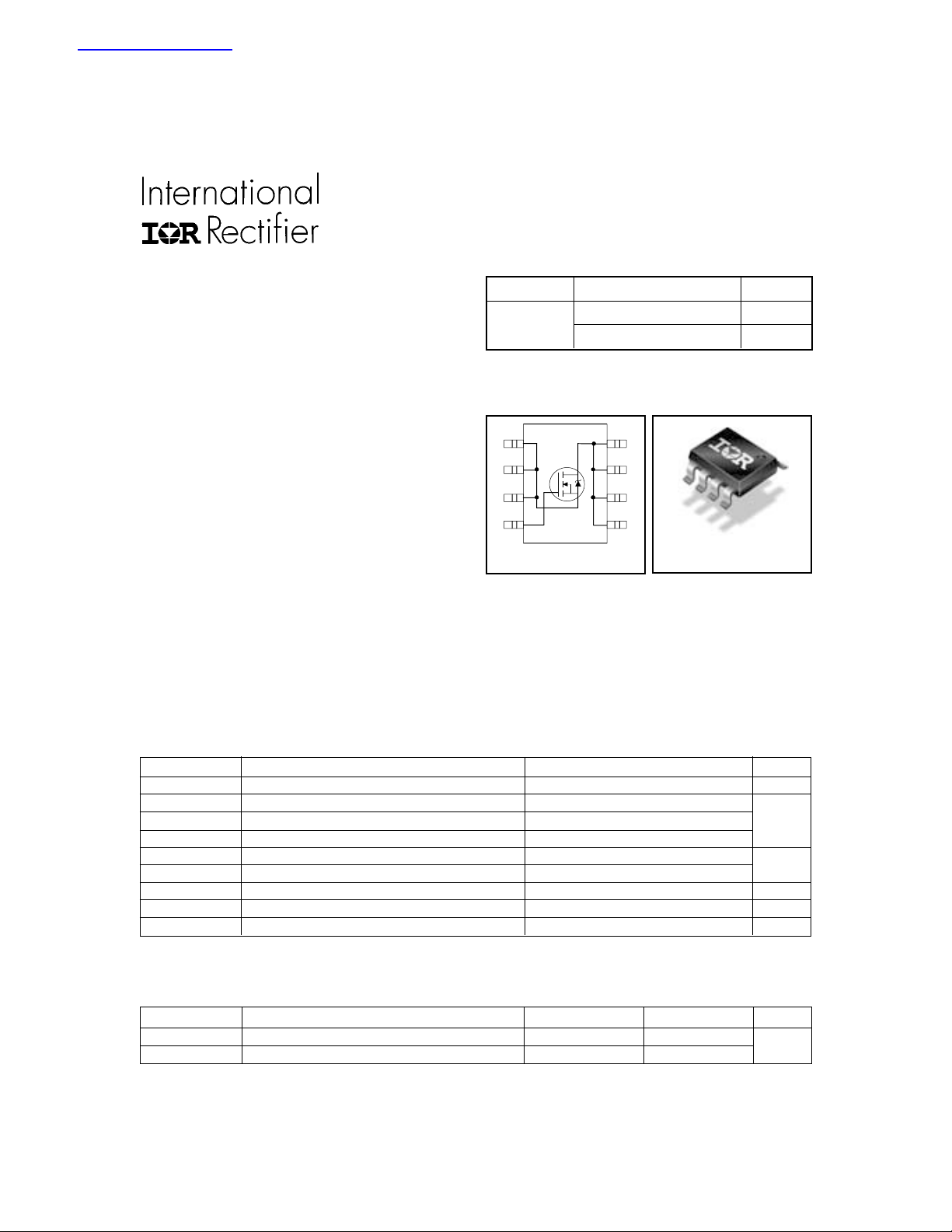
The SO-8 has been modified through a customized
Top V iew
SO-8
leadframe for enhanced thermal characteristics and
multiple-die capability making it ideal in a variety of
power applications. With these improvements, multiple
devices can be used in an application with dramatically
reduced board space. The package is designed for
vapor phase, infrared, or wave soldering techniques.
Absolute Maximum Ratings
Parameter Max. Units
V
DS
ID @ TA = 25°C Continuous Drain Current, VGS @ 4.5V 4.2
ID @ TA= 70°C Continuous Drain Current, VGS @ 4.5V 3.4 A
I
DM
PD @TA = 25°C Power Dissipation 2.5
PD @TA = 70°C Power Dissipation 1.6
V
GS
T
J, TSTG
Drain- Source Voltage 20 V
Pulsed Drain Current 17
Linear Derating Factor 0.02 mW/°C
Gate-to-Source Voltage ± 12 V
Junction and Storage Temperature Range -55 to + 150 °C
W
Thermal Resistance
Symbol Parameter Typ. Max. Units
R
θJL
R
θJA
Junction-to-Drain Lead ––– 20
Junction-to-Ambient ––– 50 °C/W
www.irf.com 1
11/15/01
IRF1902
Electrical Characteristics @ TJ = 25°C (unless otherwise specified)
Parameter Min. Typ. Max. Units Conditions
V
(BR)DSS
∆V
(BR)DSS
R
DS(on)
V
GS(th)
g
fs
I
DSS
I
GSS
Q
g
Q
gs
Q
gd
t
d(on)
t
r
t
d(off)
t
f
C
iss
C
oss
C
rss
Drain-to-Source Breakdown Voltage 20 ––– ––– VVGS = 0V, ID = 250µA
/∆T
Breakdown Voltage Temp. Coefficient ––– 0.019 ––– V/°C Reference to 25°C, ID = 1mA
J
Static Drain-to-Source On-Resistance
––– ––– 85 VGS = 4.5V, ID = 4.0A
––– ––– 170 VGS = 2.7V, ID = 3.2A
mΩ
Gate Threshold Voltage 0.70 ––– ––– VVDS = VGS, ID = 250µA
Forward Transconductance 5.6 ––– ––– SVDS = 10V, ID = 4.0A
Drain-to-Source Leakage Current
Gate-to-Source Forward Leakage ––– ––– 100 V
Gate-to-Source Reverse Leakage ––– ––– -100 VGS = -12V
––– ––– 1.0 VDS = 16V, VGS = 0V
––– ––– 25 VDS = 16V, VGS = 0V, TJ = 70°C
µA
nA
GS
= 12V
Total Gate Charge ––– 5.0 7.5 ID = 4.2A
Gate-to-Source Charge ––– 1.2 ––– nC VDS = 10V
Gate-to-Drain ("Miller") Charge ––– 1.8 ––– VGS = 4.5V
Turn-On Delay Time ––– 5.9 ––– VDD = 10V
Rise Time ––– 13 ––– ID = 1.0A
Turn-Off Delay Time ––– 23 ––– RG = 53Ω
ns
Fall Time ––– 19 ––– VGS = 4.5V
Input Capacitance ––– 310 ––– VGS = 0V
Output Capacitance ––– 130 ––– pF VDS = 15V
Reverse Transfer Capacitance ––– 55 ––– ƒ = 1.0MHz
Source-Drain Ratings and Characteristics
Parameter Min. Typ. Max. Units Conditions
I
S
I
SM
V
SD
t
rr
Q
rr
Continuous Source Current MOSFET symbol
(Body Diode) showing the
Pulsed Source Current integral reverse
(Body Diode) p-n junction diode.
–––
–––
–––
–––
4.2
17
A
G
Diode Forward Voltage ––– ––– 1.2 V TJ = 25°C, IS = 2.5A, VGS = 0V
Reverse Recovery Time ––– 38 57 ns TJ = 25°C, IF = 2.5A
Reverse Recovery Charge ––– 42 63 nC di/dt = 100A/µs
Notes:
Repetitive rating; pulse width limited by
Surface mounted on 1 in square Cu board
max. junction temperature.
Pulse width ≤ 400µs; duty cycle ≤ 2%.
2 www.irf.com
D
S
IRF1902
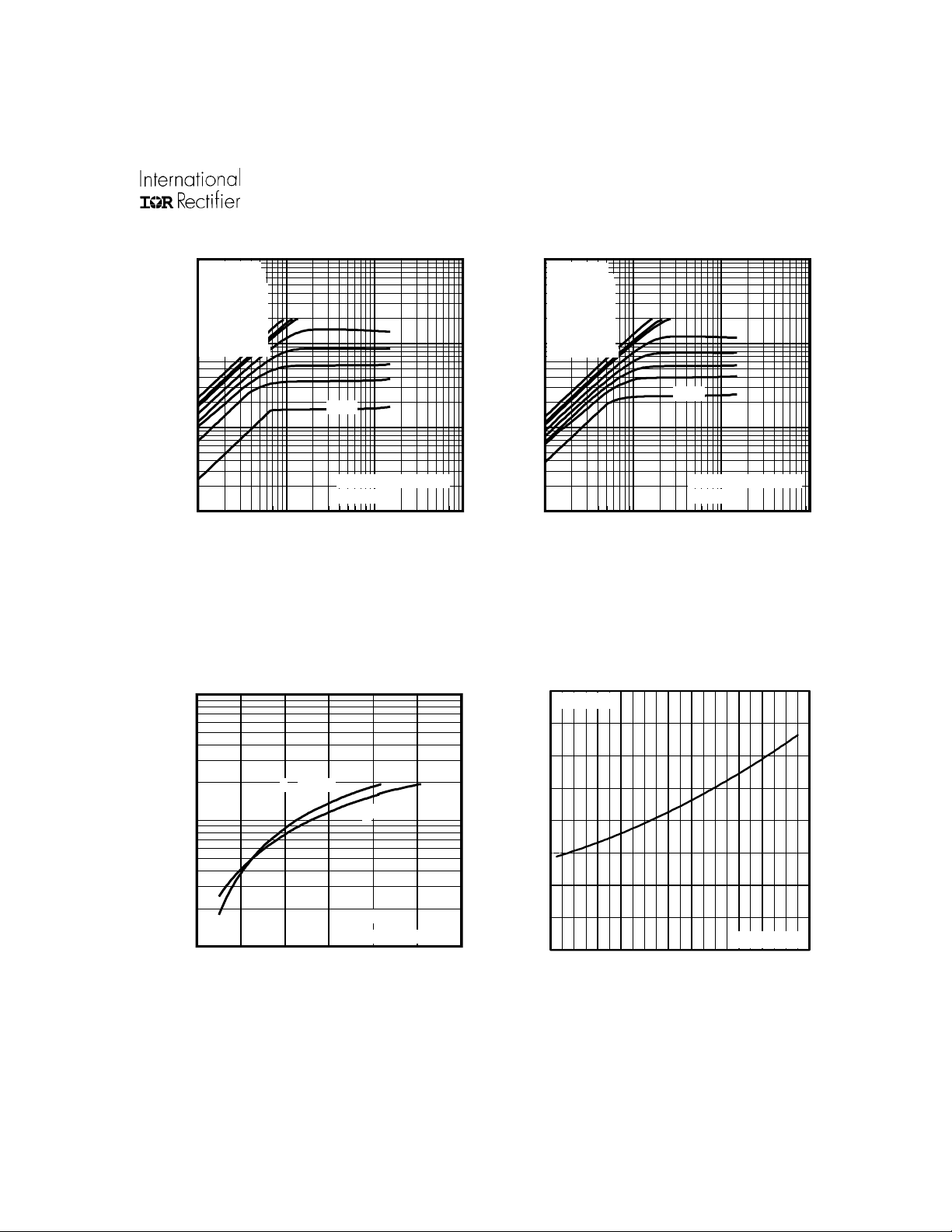
100
10
VGS
TOP 7.0V
5.0V
4.5V
3.5V
3.0V
2.7V
2.5V
BOTTOM 2.25V
2.25V
1
, Drain-to-Source Current (A)
D
I
20µs PULSE WIDTH
Tj = 25°C
0.1
0.1 1 10 100
VDS, Drain-to-Source Voltage (V)
Fig 1. Typical Output Characteristics
100.00
100
10
VGS
TOP 7.0V
5.0V
4.5V
3.5V
3.0V
2.7V
2.5V
BOTTOM 2.25V
2.25V
1
, Drain-to-Source Current (A)
D
I
20µs PULSE WIDTH
Tj = 150°C
0.1
0.1 1 10 100
VDS, Drain-to-Source Voltage (V)
Fig 2. Typical Output Characteristics
2.0
4.2A
I =
D
)
(Α
1.5
TJ = 25°C
10.00
, Drain-to-Source Current
D
I
1.00
2.0 2.5 3.0 3.5 4.0 4.5 5.0
VGS, Gate-to-Source Voltage (V)
Fig 3. Typical Transfer Characteristics
TJ = 175°C
V
= 15V
DS
20µs PULSE WIDTH
1.0
(Normalized)
0.5
DS(on)
R , Drain-to-Source On Resistance
0.0
-60 -40 -20 0 20 40 60 80 100 120 140 160
T , Junction Temperature ( C)
J
Fig 4. Normalized On-Resistance
V =
4.5V
GS
°
Vs. Temperature
www.irf.com 3

IRF1902
)
10000
1000
V
= 0V, f = 1 MHZ
GS
C
= C
iss
gs
C
= C
rss
gd
C
= C
ds
+ C
oss
+ Cgd, C
gd
Ciss
100
C, Capacitance(pF)
Coss
Crss
10
1 10 100
VDS, Drain-to-Source Voltage (V)
Fig 5. Typical Capacitance Vs.
Drain-to-Source Voltage
100.00
SHORTED
ds
6
D
I =
4.0A
V = 16V
DS
V = 10V
5
4
2
1
GS
V , Gate-to-Source Voltage (V)
0
0 1 2 4 5 6
Q , Total Gate Charge (nC
G
DS
Fig 6. Typical Gate Charge Vs.
Gate-to-Source Voltage
100
OPERATION IN THIS AREA
LIMITED BY RDS(on)
10.00
TJ = 150°C
1.00
, Reverse Drain Current (A)
SD
I
0.10
0.0 0.5 1.0 1.5
VSD, Source-toDrain Voltage (V)
Fig 7. Typical Source-Drain Diode
TJ = 25°C
V
GS
= 0V
10
100µsec
1msec
1
10msec
, Drain-to-Source Current (A)
D
I
Tc = 25°C
Tj = 150°C
Single Pulse
0.1
1 10 100
V
, Drain-toSource Voltage (V)
DS
Fig 8. Maximum Safe Operating Area
Forward Voltage
4 www.irf.com

IRF1902
(
)
5.0
4.0
3.0
2.0
D
I , Drain Current (A)
1.0
0.0
25 50 75 100 125 150
T , Case Temperature
C
°
C
Fig 9. Maximum Drain Current Vs.
Case Temperature
100
R
V
DS
V
GS
R
G
V
GS
Pulse Width ≤ 1 µs
Duty Factor ≤ 0.1 %
D
D.U.T.
Fig 10a. Switching Time Test Circuit
V
DS
90%
10%
V
GS
t
d(on)tr
t
d(off)tf
Fig 10b. Switching Time Waveforms
+
V
DD
-
D = 0.50
thJA
Thermal Response (Z )
0.20
10
0.10
0.05
P
0.02
1
0.01
SINGLE PULSE
(THERMAL RESPONSE)
Notes:
1. Duty factor D = t / t
2. Peak T = P x Z + T
0.1
0.00001 0.0001 0.001 0.01 0.1 1 10
t , Rectangular Pulse Duration (sec)
1
J DM thJA A
DM
t
1 2
1
t
2
Fig 11. Typical Effective Transient Thermal Impedance, Junction-to-Ambient
www.irf.com 5

IRF1902
)
0.15
Ω
0.14
0.13
0.12
0.11
0.10
0.09
0.08
0.07
, Drain-to -Source On Resistance (
0.06
0.05
DS(on)
0.04
R
2.0 4.0 6.0 8.0
V
GS,
ID = 4.2A
Gate -to -Source Voltage (V)
Fig 12. Typical On-Resistance Vs. Gate
Voltage
)
3.000
Ω
2.500
2.000
V
GS
= 2.7V
1.500
1.000
, Drain-to-Source On Resistance (
0.500
V
= 4.5V
DS (on)
R
0.000
GS
0 5 10 15 20
ID , Drain Current (A)
Fig 13. Typical On-Resistance Vs. Drain
Current
Current Regulator
Same Type as D.U.T.
Q
G
V
GS
Q
GS
V
G
Q
GD
Charge
Fig 14a. Basic Gate Charge Waveform
12V
V
GS
Fig 14b. Gate Charge Test Circuit
50KΩ
.2µF
.3µF
3mA
Current Sampling Resistors
+
V
D.U.T.
I
G
I
DS
-
D
6 www.irf.com

IRF1902
2.0
1.5
1.0
Gate threshold Voltage (V)
GS(th)
V
0.5
-75 -50 -25 0 25 50 75 100 125 150
TJ , Temperature ( °C )
ID = 250µA
Fig 15. Typical Threshold Voltage Vs.
Junction Temperature
50
40
30
20
Power (W)
10
0
1.00 10.00 100.00 1000.00
Time (sec)
Fig 16. Typical Power Vs. Time
www.irf.com 7

IRF1902
SO-8 Package Details
D B
8X b
5
65
4312
e1
A1
H
0.25 [.010]
A
A
C
0.10 [.004]
A
87
6
E
e
6X
0.25 [.010] C A B
NOTES:
1. DIMENSIONING & TOLERANCING PER ASME Y14.5M-1994.
2. CONTROLLING DIMENSION: MILLIMETER
3. DIMENSIONS ARE SHOWN IN MILLIMETERS [INCHES].
4. OUT L INE CONF ORMS T O JEDEC OUT L INE MS-012AA.
5 DIMENSION DOES NOT INCLUDE MOLD PROTRUS IONS.
MOLD PROTRUS IONS NOT TO EXCEED 0.15 [.006].
6 DIMENSION DOES NOT INCLUDE MOLD PROTRUS IONS.
MOLD PROTRUS IONS NOT TO EXCEED 0.25 [.010].
7 DIMENSION IS THE LENGTH OF LEAD FOR SOLDERING TO
A SUBSTRATE.
y
3X 1.27 [.05 0]
DIM
MIN MAX
A
.0532
A1
b
c .0075 .0098 0.19 0.25
D
E
e
e1
H
K
L
y
K x 45°
8X L
7
6.46 [.255]
.0688
.0040
.0098
.013
.020
.189
.1968
.1497
.1574
.050 BASIC
.025 BASIC 0.635 BASIC
.2284
.2440
.0099
.0196
.016
.050
0°
8°
8X c
FOOT PRINT
8X 0.72 [.02 8]
MILLIMETERSINCHES
MIN MAX
1.35
1.75
0.10
0.25
0.33
0.51
4.80
5.00
3.80
4.00
1.27 BASIC
5.80
6.20
0.25
0.50
0.40
1.27
0°
8°
8X 1.78 [.07 0]
SO-8 Part Marking
EXAMPLE: THIS IS AN IRF7101 (MOSFET)
DATE CODE (YWW)
Y = LAST DIGIT O F THE YEAR
YW W
XXXX
INTER NATIONAL
F7101
RECT IFIER
LOGO
8 www.irf.com
WW = WEEK
LOT CODE
PART NUM BER

(
)
)
)
)
)
)
)
SO-8 Tape and Reel
TERMINAL NUMBER 1
12.3 ( .484
11.7 ( .461
IRF1902
8.1 ( .318
7.9 ( .312
NOTES:
1. CONTROLLING DIMENSION : M ILLIMETER.
2. ALL DIM ENSIONS ARE SHOWN IN MILLIMETERS(INCHES).
3. OU TLIN E C O N FORM S TO EIA-481 & EIA-541.
330. 00
12.992
MAX.
NOTES :
1. CONTRO LLING DIMENSION : MILLIMETER.
2. OU TL INE CO N FO R M S T O EIA-481 & EIA-541.
Data and specifications subject to change without notice.
This product has been designed and qualified for the Industrial market.
Qualification Standards can be found on IR’s Web site.
FEED DIRECTION
14.40 ( .5 6 6
12.40 ( .4 8 8
IR WORLD HEADQUARTERS: 233 Kansas St., El Segundo, California 90245, USA Tel: (310) 252-7105
TAC Fax: (310) 252-7903
Visit us at www.irf.com for sales contact information.11/01
www.irf.com 9
 Loading...