PD-97392
SupIRBuck
TM
10A HIGHLY INTEGRATED
IR3870MBF
WIDE-INPUT VOLTAGE, SYNCHRONOUS BUCK REGULATOR
Features
• Input Voltage Range: 3V to 26V
• Output Voltage Range: 0.5V to 12V
• Continuous 10A Load Capability
• Constant On-Time control
• Excellent Efficiency at very low output current levels
• Gate drive charge pump option to maximize
efficiency at higher output current levels
• Compensation Loop not Required
• Programmable switching frequency, soft start, and
over current protection
• Power Good Output
• Precision Voltage Reference (0.5V, +/-1%)
• Enable Input with Voltage Monitoring Capability
• Pre-bias Start Up
• Under/Over Voltage Fault Protection
• Ultra small, low profile 5 x 6mm QFN Package
• Lead-free, halogen-free and RoHS compliant
Applications
• Notebook and desktop computers
• Game consoles
• Consumer electronics - STB, LCD TV, Printers
• General purpose POL DC-DC Converters
Description
The IR3870M SupIRBuck
fully integrated and highly efficient DC/DC
voltage regulator. The onboard constant on time
hysteretic controller and MOSFETs make IR3870
a space-efficient solution that delivers up to 10A
of precisely controlled output voltage in 60°C
ambient temperature applications without airflow.
Programmable switching frequency, soft start,
and over current protection allows for a very
flexible solution suitable for many different
applications. The combination of the gate drive
charge pump option and constant on time control
allow efficiency optimization in the whole output
current range, making this device an ideal choice
for battery powered applications.
Additional features include pre-bias startup, very
precise 0.5V reference, over/under voltage shut
down, power good output, and enable input with
voltage monitoring capability.
TM
is an easy-to-use,
1/27/2010
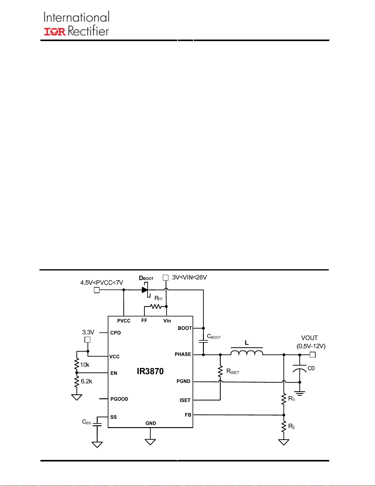
Typical Notebook Application Circuit Diagram
1
IR3870MBF
ABSOLUTE MAXIMUM RATINGS
(Voltages referenced to GND unless otherwise specified)
• VIN ……………………………………………………. 30V
• VCC ……………….….………………………………. 3.9V
• PVCC ……………….….…………….……..………… 7.5V
• Boot ……………………………………..……….….. 40V
• PHASE …………………………………………..…….. -0.3V to 30V(DC), -5V(100ns)
• Boot to PHASE…..…………………………….…..…… 7.5V
• FF ………………………………………….………… 30V
• PGND to GND ……………...…………………………. -0.3V to +0.3V
• All other pins ……………...…………………………… 3.9V
• Storage Temperature Range ..................................... -65°C To 150°C
• Junction Temperature Range .................................... -10°C To 150°C
• ESD Classification …………………………….……… JEDEC Class 1C
• Moisture sensitivity level………………...…………….. JEDEC Level 3@260 °C
Stresses beyond those listed under “Absolute Maximum Ratings” may cause permanent damage to the
device. These are stress ratings only and functional operation of the device at these or any other
conditions beyond those indicated in the operational sections of the specifications are not implied.
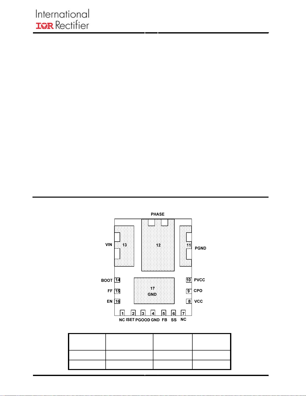
PACKAGE INFORMATION
5mm x 6mm POWER QFN
=
JA
=
-
PCBJ
o
W/C35θ
o
W/C2θ
ORDERING INFORMATION
PKG DESIG
M
PACKAGE
DESCRIPTION
IR3870MTRPbF
PIN COUNT
23
PARTS PER
REEL
4000
75023IR3870MTR1PbFM
2
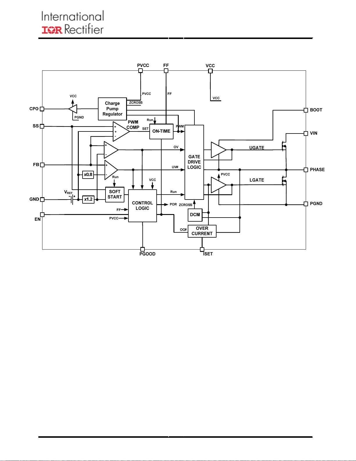
Block Diagram
IR3870MBF
3
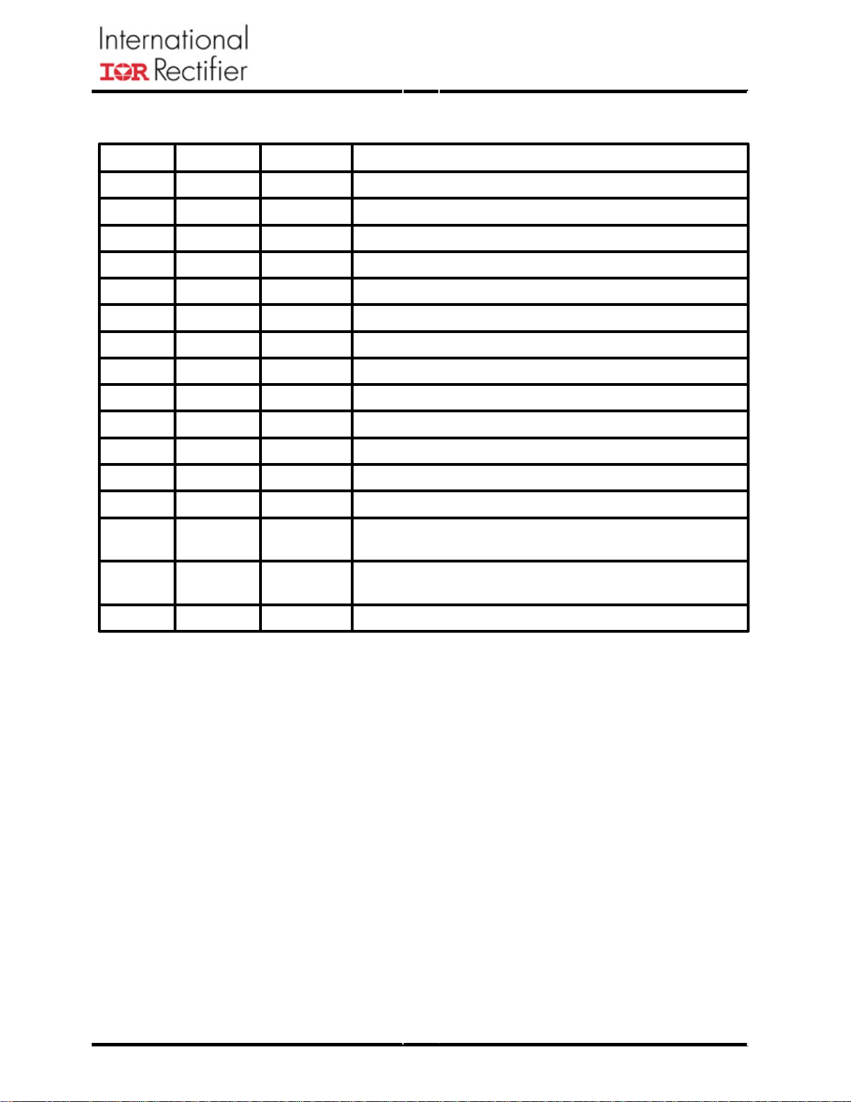
Pin Description
DESCRIPTIONI/O LEVELNUMBERNAME
No connection1NC
Connecting resistor to PHASE pin sets over current trip point2ISET
Power good – pull up to 5V5V3PGOOD
Bias return and signal referenceReference4,17GND
Inverting pin of PWM comparator and OVP/PGood sense3.3V5FB
Set soft start slew-rate with a capacitor to GND 3.3V6SS
No connection7NC
Internal bias supply3.3V8VCC
Charge pump output0.75V9CPO
Gate drive supply5V10PVCC
Power returnReference11PGND
Phase node (or switching node) of MOSFET half bridgeVIN12PHASE
IR3870MBF
Input voltage for the system.VIN13VIN
14BOOT
VIN
+PVCC
VIN15FF
Bootstrapped gate drive supply – connect a capacitor to
PHASE
Input voltage feed forward – sets on-time with a resistor to
VIN
Enable – turns device on or off5V16EN
4
IR3870MBF
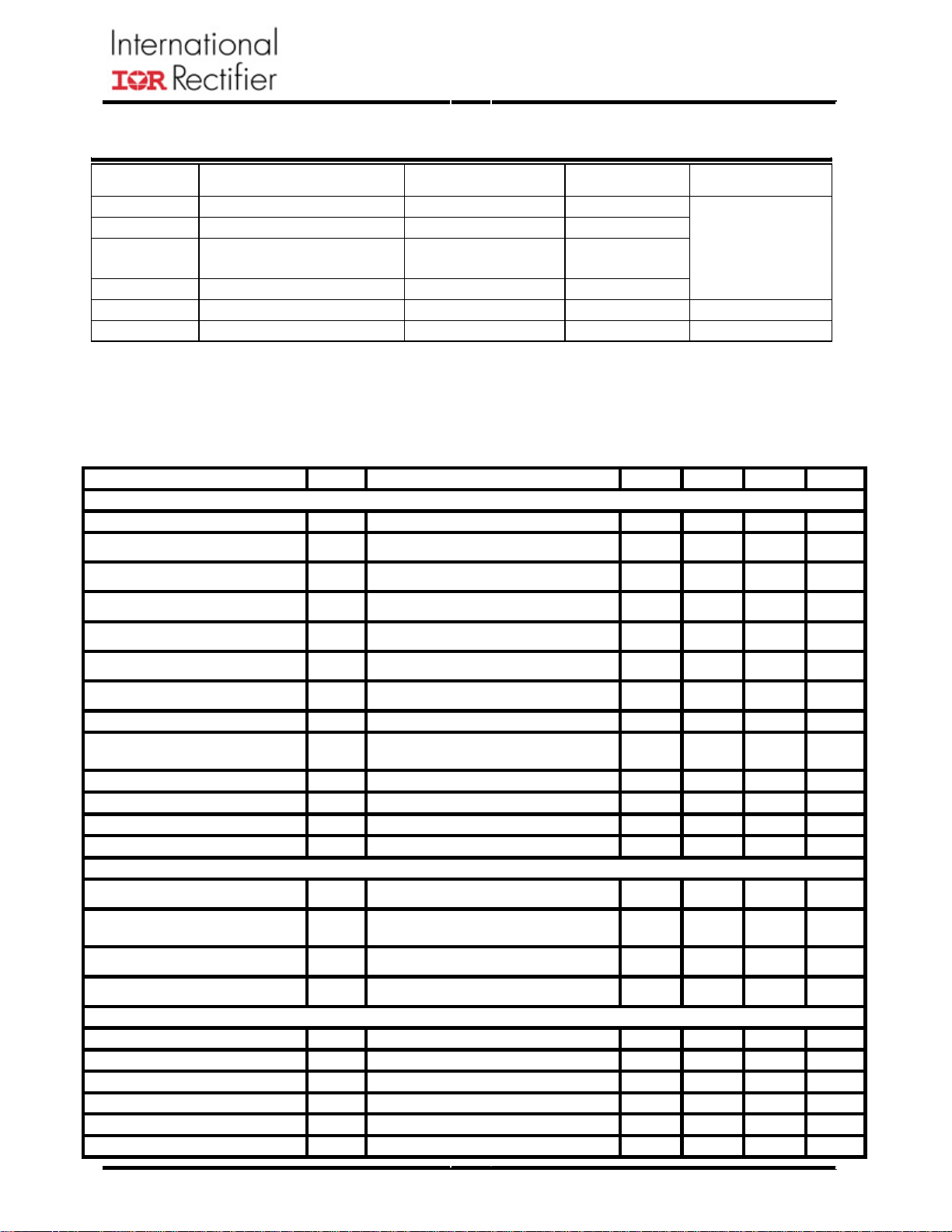
Recommended Operating Conditions
Symbol Definition Min Max Units
VIN Input Voltage 3 26*
VCC Supply Voltage 3 3.6
Boot to
Supply Voltage 7.0
PHASE
V
Output Voltage 0.5 12
OUT
I
Output Current 0 10 A
OUT
Fs Switching Frequency 1000 kHz
* Note: PHASE pin must not exceed 30V.
Electrical Specifications
Unless otherwise specified, these specification apply over VIN = 12V, PVCC = 7VDC, 0oC ≤ TJ≤ 125oC.
PARAMETER NOTE TEST CONDITION MIN TYP MAX UNIT
BIAS SUPPLIES
VCC Turn-on Threshold 3 V
VCC Turn-off Threshold
VCC Threshold Hysteresis
PVCC Turn-on Threshold
PVCC Turn-off Threshold
PVCC Threshold Hysteresis
VCC Shutdown Current
VCC Operating Current RFF = 180k, EN = HIGH 1.2 mA
PVCC Operating Current RFF = 180k,
PVCC Shutdown Current EN=LOW 20 60
FF Shutdown Current EN=LOW 0.1 2
VIN Shutdown Current EN=LOW 0 1
PHASE Shutdown Current EN=LOW 0.25 2
CONTROL LOOP
Reference Accuracy, V
On-Time Accuracy
Min Off Time
Soft-Start Current
FAULT PROTECTION
ISET pin output current 18 20 22
Under Voltage Threshold Falling VFB & monitor PGOOD 0.37 0.4 0.43 V
Under Voltage Hysteresis Rising VFB 7.5 mV
Over Voltage Threshold Rising VFB & monitor PGOOD 0.56 0.6 0.64 V
Over Voltage Hysteresis 1 Rising VFB 7.5 mV
PGOOD Delay Threshold (VSS) 0.6 V
REF
EN=LOW 30 60
EN = HIGH, Fs = 500kHz
R
= 180 k, TJ = 650C
FF
EN = HIGH
2.65 V
60 mV
3.05 V
2.65 V
60 mV
8 mA
0.495 0.5 0.505 V
280 300 320 ns
300 ns
8 10 12
V
μA
μA
μA
μA
μA
μA
μA
5
IR3870MBF
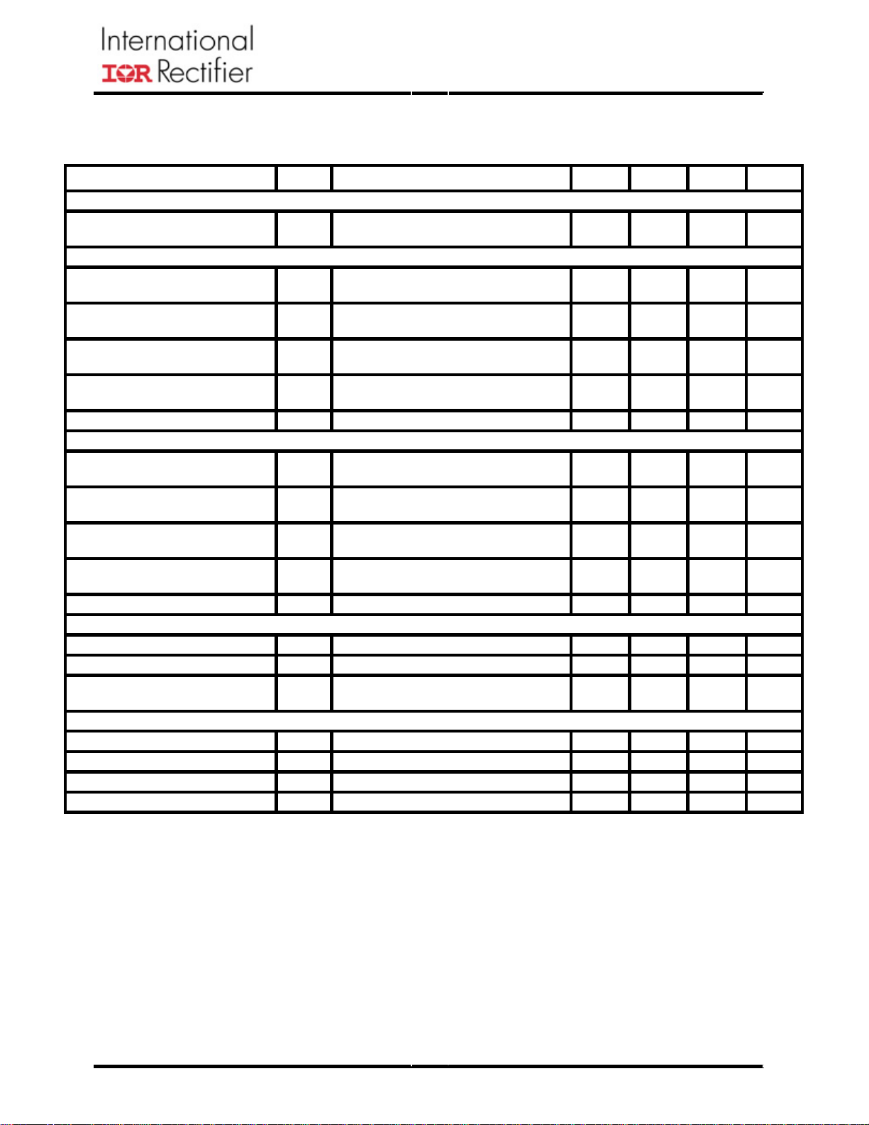
Electrical Specifications (continued)
Unless otherwise specified, these specification apply over VIN = 12V, PVCC = 7VDC, 0oC ≤ TJ ≤ 125oC.
PARAMETER NOTE TEST CONDITION MIN TYP MAX UNIT
GATE DRIVE
Dead time 1 Monitor body diode conduction on
PHASE pin
UPPER MOSFET
Static Drain-to-Source On-
PVCC =5V, ID =10A, TJ =25oC 14.7 m
Resistance
Static Drain-to-Source On-
PVCC =5V, ID =10A, TJ =125oC 26 m
Resistance
Static Drain-to-Source On-
PVCC =7V, ID =10A, TJ =25oC 11.9 m
Resistance
Static Drain-to-Source On-
PVCC =7V, ID =10A, TJ =125oC 22 m
Resistance
Diode Forward Voltage VGS =0V, IS =10A, TJ =25oC 1.0 V
LOWER MOSFET
Static Drain-to-Source On-
PVCC =5V, ID =10A, TJ =25oC 6.2 m
Resistance
Static Drain-to-Source On-
PVCC =5V, ID =10A, TJ =125oC 11 m
Resistance
Static Drain-to-Source On-
PVCC =7V, ID =10A, TJ =25oC 5.1 m
Resistance
Static Drain-to-Source On-
PVCC =7V, ID =10A, TJ =125oC 9 m
Resistance
Diode Forward Voltage VGS =0V, IS =10A, TJ =25oC 1.0 V
CHARGE PUMP OUTPUT
Source Resistance I
Sink Resistance I
Charge Pump Disable
Threshold, V
CP TH
6.7 7.2 V
=15mA 3.3 5
CPO
=15mA 1 2.1
CPO
LOGIC INPUT AND OUTPUT
EN Rising Threshold 1.13 1.21 1.29 V
EN Hysteresis 40 100 160 mV
EN Input Current 1
PGOOD pull down resistance I
=2mA 50 100
PGOOD
Notoe1: Guaranteed by design, not tested in production
5 30 ns
μA
6
 Loading...