Data Sheet No. 94715
IR3637ASPbF
1% ACCURATE SYNCHRONOUS PWM CONTROLLER
FEATURES
0.8V Reference Voltage
Operates with a single 5V Supply
Internal 600KHz Oscillator
Soft-Start Function
Fixed Frequency Voltage Mode
Short Circuit Protection
APPLICATIONS
Computer Peripheral Voltage Regulator
Memory Power supplies
Graphics Card
Low cost on-board DC to DC
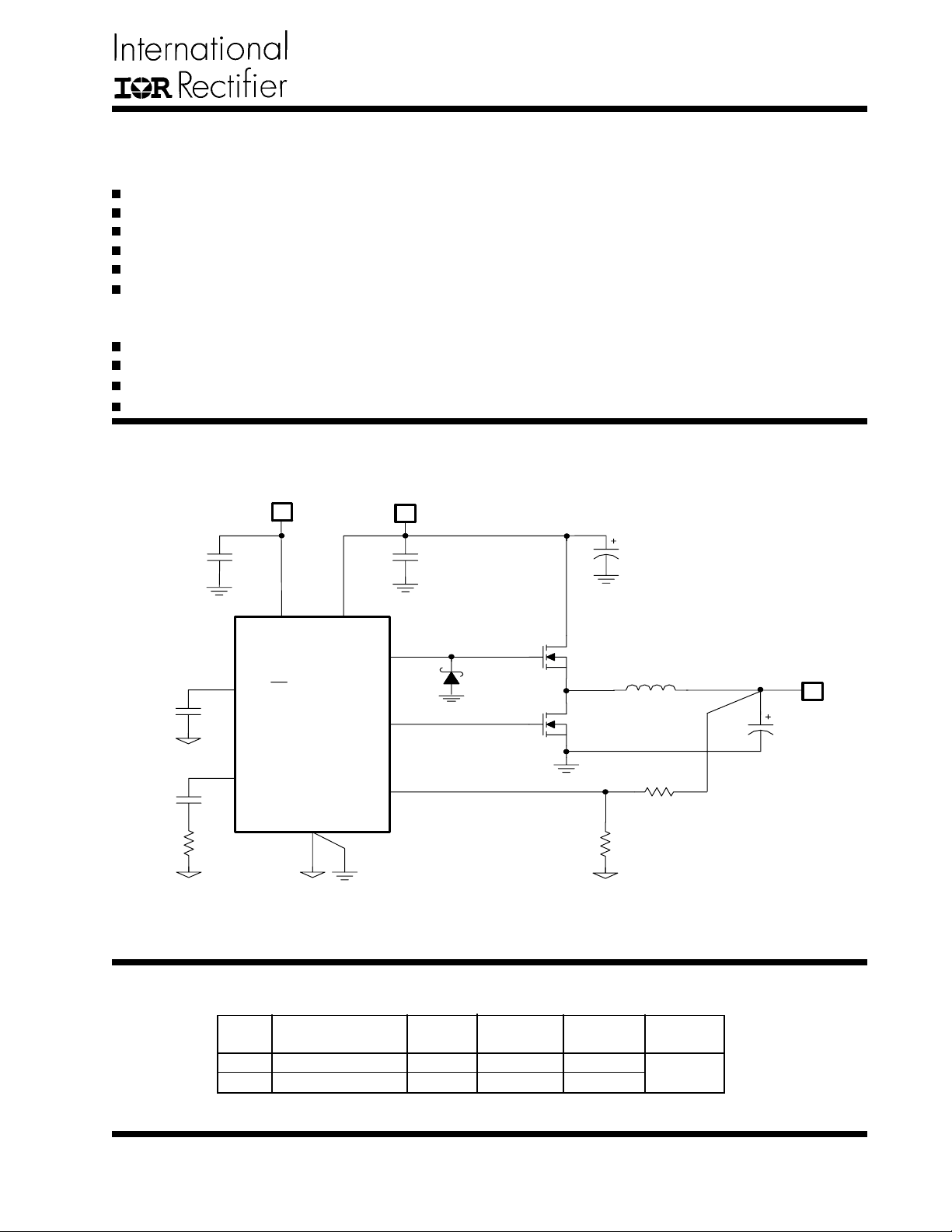
TYPICAL APPLICATION
12V
C3
5V
C2
DESCRIPTION
The IR3637A controller IC is designed to provide a simple
synchronous Buck regulator for on-board DC to DC applications in a small 8-pin SOIC. The output voltage can
be precisely regulated using the internal 0.8V reference
voltage for low voltage applications.
The IR3637A operates at a fixed internal 600KHz switching frequency to reduce the component size.
The device features under-voltage lockout for both input
supplies, an external programmable soft-start function
as well as output under-voltage detection that latches
off the device when an output short is detected.
C1
C4
C5
R1
Vc Vcc
Q1
L1
Q2
SS/SD
HDrv
D1
LDrv
IR3637A
Comp
Fb
Gnd
Figure 1 - Typical application of IR3637A.
R3
R2
ORDERING INFORMATION
PKG PACKAGE PIN PARTS PARTS T & R
DESIG DESCRIPTION COUNT PER TUBE PER REEL Oriantation
S IR3637ASPbF 8 95 ----- S IR3637ASTRPbF 8 ------- 2500
Fig A
Vout
C6
www.irf.com
1
IR3637ASPbF
ABSOLUTE MAXIMUM RATINGS
Vcc Supply Voltage ................................................ 16V
Vc Supply Voltage .................................................. 25V
Storage Temperature Range ..................................... -65°C To 150°C
Operating Junction Temperature Range ..................... 0°C To 125°C
ESD Classification ................................................. HBM Class 2 (2KV) JEDEC Standard
Moisture Sensitivity Level ........................................ JEDEC Level 1 @ 260°C
CAUTION: Stresses above those listed in "Absolute Maximum Ratings" may cause permanent damage to the device.
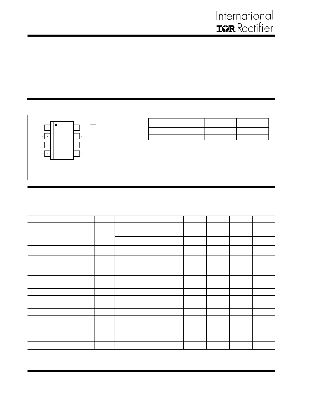
PACKAGE INFORMATION
Recommended Operating Conditions
1
Fb
2
Vcc
3
LDrv
4
Gnd HDrv
θJA=154°C/W
θJC=41.2°C/W
8
7
6
5
SS/SD
Comp
Vc
Parameter Min Max Units
Vcc 4.5 5.5 V
Vc 8 14 V
ELECTRICAL SPECIFICATIONS
Unless otherwise specified, these specifications apply over Vcc=5V, Vc=12V and 0°C<Tj<125°C.
PARAMETER SYM TEST CONDITION MIN TYP MAX UNITS
Feedback Voltage
Fb Voltage
Fb Voltage Line Regulation
UVLO
UVLO Threshold - Vcc
UVLO Hysteresis - Vcc
UVLO Threshold - Vc
UVLO Hysteresis - Vc
UVLO Threshold - Fb
Supply Current
Vcc Dynamic Supply Current
Vc Dynamic Supply Current
Vcc Static Supply Current
Vc Static Supply Current
Soft-Start Section
Charge Current
Shutdown Threshold
VFB
LREG
UVLO Vcc
UVLO Vc
UVLO Fb
Dyn Icc
Dyn Ic
ICCQ
ICQ
SSIB
SD
25°C<Tj<75°C
0°C<Tj<125°C
4.5<Vcc<5.5
Supply Ramping Up
Supply Ramping Up
Fb Ramping Down
Freq=600KHz, CL=1500pF
Freq=600KHz, CL=1500pF
SS=0V
SS=0V
SS=0V
0.792
0.789
4.0
3.1
0.3
4
6
1
0.5
-15
0.800
0.800
4.2
0.25
3.3
0.2
0.4
7
15
3.3
1
-25
0.808
0.811
0.1
4.4
3.5
0.5
16
20
6
4.7
-35
0.4
V
V
%
V
V
V
V
V
mA
mA
mA
mA
µA
V
2
www.irf.com
IR3637ASPbF
PARAMETER SYM TEST CONDITION MIN TYP MAX UNITS
Error Amp
Fb Voltage Input Bias Current
Fb Voltage Input Bias Current
Transconductance
Oscillator
Frequency
SS=3V, Fb=0.6V
IFB1
SS=0V, Fb=0.6V
IFB2
gm
Freq
450
540
-0.1
-64
600
600
800
660
µA
µA
µmho
KHz
Ramp-Amplitude Voltage
V
RAMP
Output Drivers
Rise Time, Hdrv, Ldrv
Fall Time,Hdrv, Ldrv
Dead Band Time
Max Duty Cycle
Min Duty Cycle
CL=1500pF, Vcc=12V,2V to 9V
Tr
C
Tf
TDB
TON
TOFF
L=1500pF, Vcc=12V, 9V to 2V
Vcc=12V, 2V to 2V
Fb=0.6V, Freq=600KHz
Fb=1V
PIN DESCRIPTIONS
PIN# PIN SYMBOL PIN DESCRIPTION
1
2
3
4
Fb
Vcc
LDrv
Gnd
This pin is connected directly to the output of the switching regulator via resistor divider to
set the output voltage and provide feedback to the error amplifier.
This pin provides biasing for the internal blocks of the IC as well as powers the low side
driver. A minimum of 0.1µF, high frequency capacitor must be connected from this pin to
ground to provide peak drive current capability.
Output driver for the synchronous power MOSFET.
IC's ground pin, this pin must be connected directly to the ground plane. A high frequency
capacitor (0.1 to 1µF) must be connected from Vcc and Vc pins to this pin for noise free
operation.
40
76
1.25
30
30
150
60
60
200
V
ns
ns
ns
%
0
0
%
5
6
7
8
www.irf.com
HDrv
Vc
Comp
SS / SD
Output driver for the high side power MOSFET. The negative voltage at this pin may cause
instability for the gate drive circuit. To prevent this, a low forward voltage drop diode (e.g.
BAT54 or 1N4148) is required between this pin and ground.
This pin is connected to a voltage that must be at least 4V higher than the bus voltage
(assuming 5V threshold MOSFET) and powers the high side output driver. A minimum of
0.1µF, high frequency capacitor must be connected from this pin to ground to provide
peak drive current capability.
Compensation pin of the error amplifier. An external resistor and capacitor network is
typically connected from this pin to ground to provide loop compensation.
This pin provides user programmable soft-start function. Connect an extrnal capacitor
from this pin to ground to set the start up time of the output. The converter can be shutdown by pulling this pin below 0.4V. During shutdown both drivers turn off.
3
IR3637ASPbF
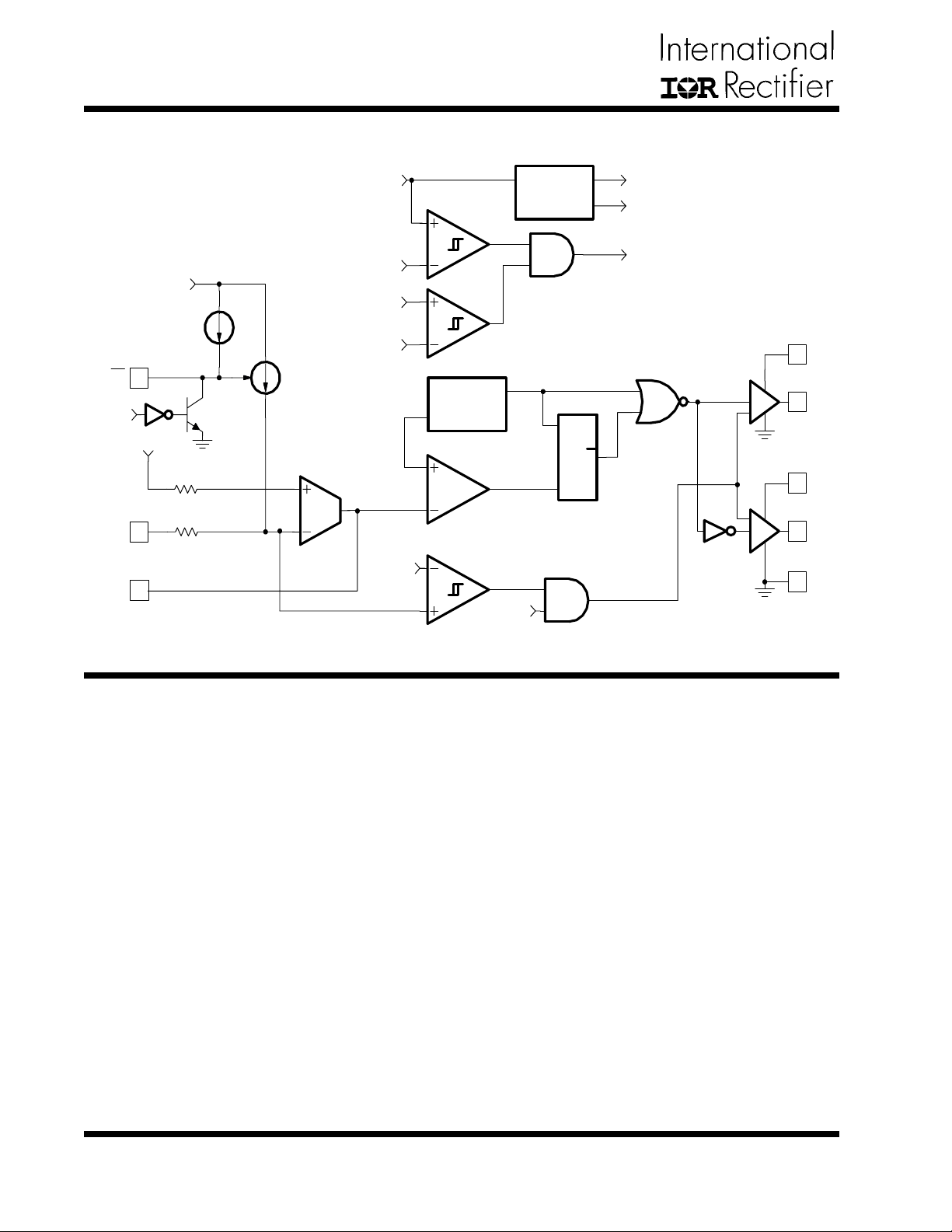
BLOCK DIAGRAM
SS/SD
POR
Fb
Comp
8
0.8V
1
7
3V
25uA
25K
25K
64uA Max
Error Amp
Vcc
4.2V
Vc
3.3V
0.4V
Ct
Oscillator
Error Comp
FbLo Comp
POR
Bias
Generator
S
R
Reset Dom
3V
0.8V
POR
6
Vc
5
HDrv
Q
2
Vcc
3
LDrv
Gnd
4
Figure 2 - Simplified block diagram of the IR3637A.
THEORY OF OPERATION
Introduction
The IR3637A is a fixed frequency, voltage mode synchronous controller and consists of a precision reference voltage, an error amplifier, an internal oscillator, a
PWM comparator, 0.5A peak gate driver, soft-start and
shutdown circuits (see Block Diagram).
The output voltage of the synchronous converter is set
and controlled by the output of the error amplifier; this is
the amplified error signal from the sensed output voltage
and the reference voltage.
This voltage is compared to a fixed frequency linear
sawtooth ramp and generates fixed frequency pulses of
variable duty-cycle, which drives the two N-channel external MOSFETs.The timing of the IC is provided through
an internal oscillator circuit which uses on-chip capacitor to set the oscillation frequency to 600 KHz.
Short-Circuit Protection
The output is protected against the short-circuit. The
IR3637A protects the circuit for shorted output by sensing the output voltage (through the external resistor divider). The IR3637A shuts down the PWM signals, when
the output voltage drops below 0.4V.
Under-Voltage Lockout
The under-voltage lockout circuit assures that the
MOSFET driver outputs remain in the off state whenever
the supply voltage drops below set parameters. Lockout
occurs if Vc or Vcc fall below 3.3V and 4.2V respectively. Normal operation resumes once Vc and Vcc rise
above the set values.
Shutdown
The converter can be shutdown by pulling the soft-start
pin below 0.4V. This can be easily done by using an
external small signal transistor. During shutdown both
drivers turn off.
4
www.irf.com
THEORY OF OPERATION
IR3637ASPbF
Soft-Start
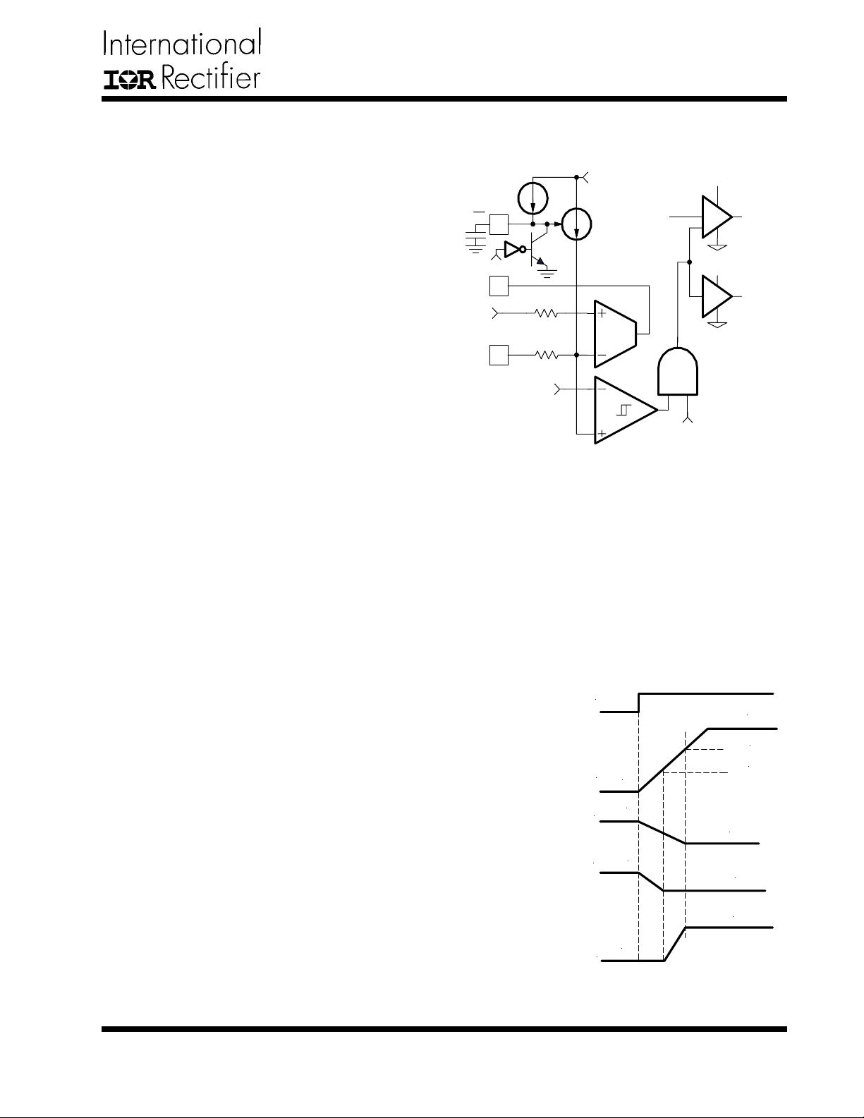
The IR3637A has a programmable soft-start to control
the output voltage rise and limit the current surge at the
start-up. To ensure correct start-up, the soft-start sequence initiates when the Vc and Vcc rise above their
threshold (3.3V and 4.2V respectively) and generates
the Power On Reset (POR) signal. Soft-start function
operates by sourcing an internal current to charge an
external capacitor to about 3V. Initially, the soft-start function clamps the E/A’s output of the PWM converter and
disables the short circuit protection. During the power
up, the output starts at zero and voltage at Fb is below
0.4V. The feedback UVLO is disabled during this time
by injecting a current (64µA) into the Fb. This generates
a voltage about 1.6V (64µA×25K) across the negative
input of E/A and positive input of the feedback UVLO
comparator (see Figure 3).
The magnitude of this current is inversely proportional to
the voltage at soft-start pin.
The 20µA current source starts to charge up the external capacitor. In the mean time, the soft-start voltage
ramps up, the current flowing into Fb pin starts to decrease linearly and so does the voltage at the positive
pin of feedback UVLO comparator and the voltage negative input of E/A.
3V
64uA
Max
Error Amp
Feeback
UVLO Comp
HDrv
LDrv
POR
SS/SD
Comp
0.8V
Fb
25uA
POR
64uA
25K
25K
0.4V
×
25K=1.6V
When SS=0
Figure 3 - Soft-start circuit for IR3637A.
The output start-up time is the time period when softstart capacitor voltage increases from 1V to 2V. The startup time will be dependent on the size of the external
soft-start capacitor. The start-up time can be estimated
by:
25µA×TSTART/CSS = 2V-1V
When the soft-start capacitor is around 1V, the current
flowing into the Fb pin is approximately 32µA. The voltage at the positive input of the E/A is approximately:
32µA×25K = 0.8V
The E/A will start to operate and the output voltage starts
to increase. As the soft-start capacitor voltage continues to go up, the current flowing into the Fb pin will keep
decreasing. Because the voltage at pin of E/A is regulated to reference voltage 0.8V, the voltage at the Fb is:
VFB = 0.8-25K×(Injected Current)
The feedback voltage increases linearly as the injecting
current goes down. The injecting current drops to zero
when soft-start voltage is around 2V and the output voltage goes into steady state.
As shown in Figure 4, the positive pin of feedback UVLO
comparator is always higher than 0.4V, therefore, feedback UVLO is not functional during soft-start.
For a given start up time, the soft-start capacitor can be
estimated as:
CSS ≅ 25µA×TSTART/1V
Output of UVLO
Current flowing
Voltage at negative input
of Error Amp and Feedback
UVLO comparator
Voltage at Fb pin
POR
Soft-Start
Voltage
into Fb pin
0V
64uA
≅
1.6V
0V
0uA
0.8V
0.8V
3V
≅
2V
≅
1V
Figure 4 - Theoretical operational waveforms
during soft-start.
www.irf.com
5
IR3637ASPbF
APPLICATION INFORMATION
Design Example:
The following example is a typical application for IR3637A.
Appliaction circuit is shown in page 12.
VIN = Vcc = 5V
Vc=12V
VOUT = 1.8V
IOUT = 6A
∆VOUT = 50mV
FS = 600KHz
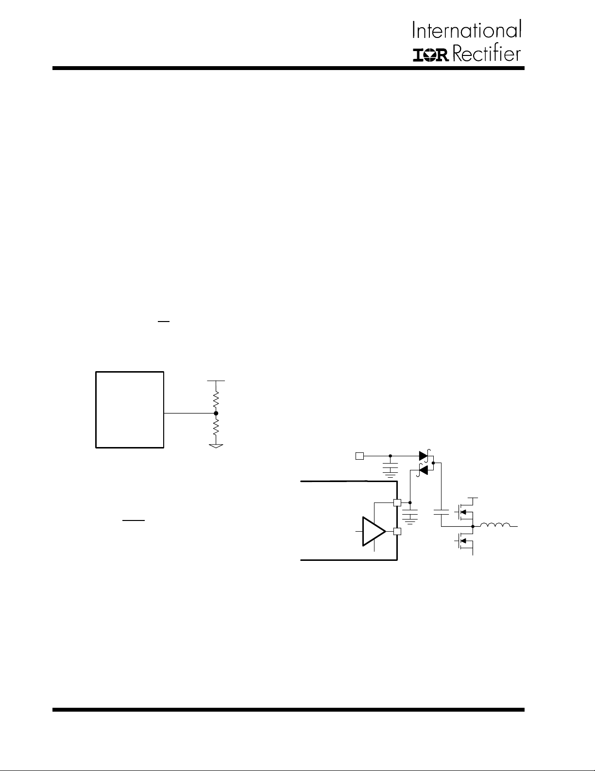
Output Voltage Programming
Output voltage is programmed by reference voltage and
external voltage divider. The Fb pin is the inverting input
of the error amplifier, which is internally referenced to
0.8V. The divider is ratioed to provide 0.8V at the Fb pin
when the output is at its desired value. The output voltage is defined by using the following equation:
R6
VOUT = VREF ×
When an external resistor divider is connected to the
output as shown in Figure 5.
1 +
( )
IR3637A
Figure 5 - Typical application of the IR3637A for
programming the output voltage.
---(1)
R5
Fb
V
OUT
6
R
R
5
Css ≅ 25×tSTART (µF) ---(2)
Where tSTART is the desired start-up time (ms)
For a start-up time of 4ms, the soft-start capacitor will
be 0.1µF. Choose a ceramic capacitor at 0.1µF.
Boost Supply for Single 5V appliaction
To drive the high side switch, it is necessary to supply a
gate voltage at least 4V grater than the bus voltage. This
is achieved by using a charge pump configuration as
shown in Figure 6. This method is simple and inexpensive. The operation of the circuit is as follows: when the
lower MOSFET is turned on, the capacitor (C1) is pulled
down to ground and charges, up to VBUS value, through
the diode (D1). The bus voltage will be added to this
voltage when upper MOSFET turns on in next cycle,
and providing supply voltage (Vc) through diode (D2). Vc
is approximately:
Vc ≅ 2VBUS - (VD1 + VD2)
Capacitors in the range of 0.1µF and 1µF are generally
adequate for most applications. The diode must be a
fast recovery device to minimize the amount of charge
fed back from the charge pump capacitor into V
diodes need to be able to block the full power rail voltage, which is seen when the high side MOSFET is
switched on. For low voltage application, schottky diodes can be used to minimize forward drop across the
diodes at start up.
BUS
V
C3
D1
D2
BUS. The
Equation (1) can be rewritten as:
VOUT
R6 = R5 ×
Choose R5 = 1KΩ
This will result to R6 = 1.25KΩ
If the high value feedback resistors are used, the input
bias current of the Fb pin could cause a slight increase
in output voltage. The output voltage set point can be
more accurate by using precision resistor.
Soft-Start Programming
The soft-start timing can be programmed by selecting
the soft-start capacitance value. The start-up time of the
converter can be calculated by using:
- 1
( )
VREF
6
BUS
C1
V
Q1
L
Q2
www.irf.com
Vc
C2
IR3637A
Figure 6 - Charge pump circuit.
Input Capacitor Selection
The input filter capacitor should be based on how much
ripple the supply can tolerate on the DC input line. The
ripple current generated during the on time of upper
MOSFET should be provided by input capacitor. The RMS
value of this ripple is expressed by:
HDrv
 Loading...