Data Sheet No. PD60233 revB
IR2277S/IR2177S(PbF)
Phase Current Sensor IC for AC motor control
Features
• Floating channel up to 600 V for IR2177 & 1200 V for
IR2277
• Synchronous sampling measurement system
• High PWM noise (ripple) rejection capability
• Digital PWM output
• Fast Over Current detection
• Suitable for bootstrap power supplies
• Low sensing latency (<7.5 µsec @20kHz)
• Ratiometric analog output suitable for DSP A/D interface
Description
IR2177/IR2277 is a high voltage, high speed, single phas e current
sensor interface for AC motor drive applications. The current is
sensed by an external shunt resistor. The IC converts the analog
voltage into a time interval through a precise circuit that also
performs a very good ripple rejection showing small group delay.
The time interval is level shifted and given to the output both as a
PWM signal (PO) and analog voltage (OUT). The anal og voltage is
proportional to the measured current and is ratio metric with respect
to an externally provided voltage reference. The max throughput is
40 ksample/sec suitable for up to 20 kHz asymmetrical PWM
modulation and max delay is <7.5
current signal is provided for IGBT protection.
µsec (@20kHz). Also a fast over
Product Summary
V
(max) IR2277 1200 V
OFFSET
IR2177 600 V
V
range ±250mV
in
Bootstrap supply range 8-20 V
Floating channel quiescent
current (max)
Sensing latency (max) 7.5 µsec
Throughput 40ksample/sec
Over Current threshold
(max)
2.2 mA
(@20kHz)
(@20kHz)
±470 mV
Package
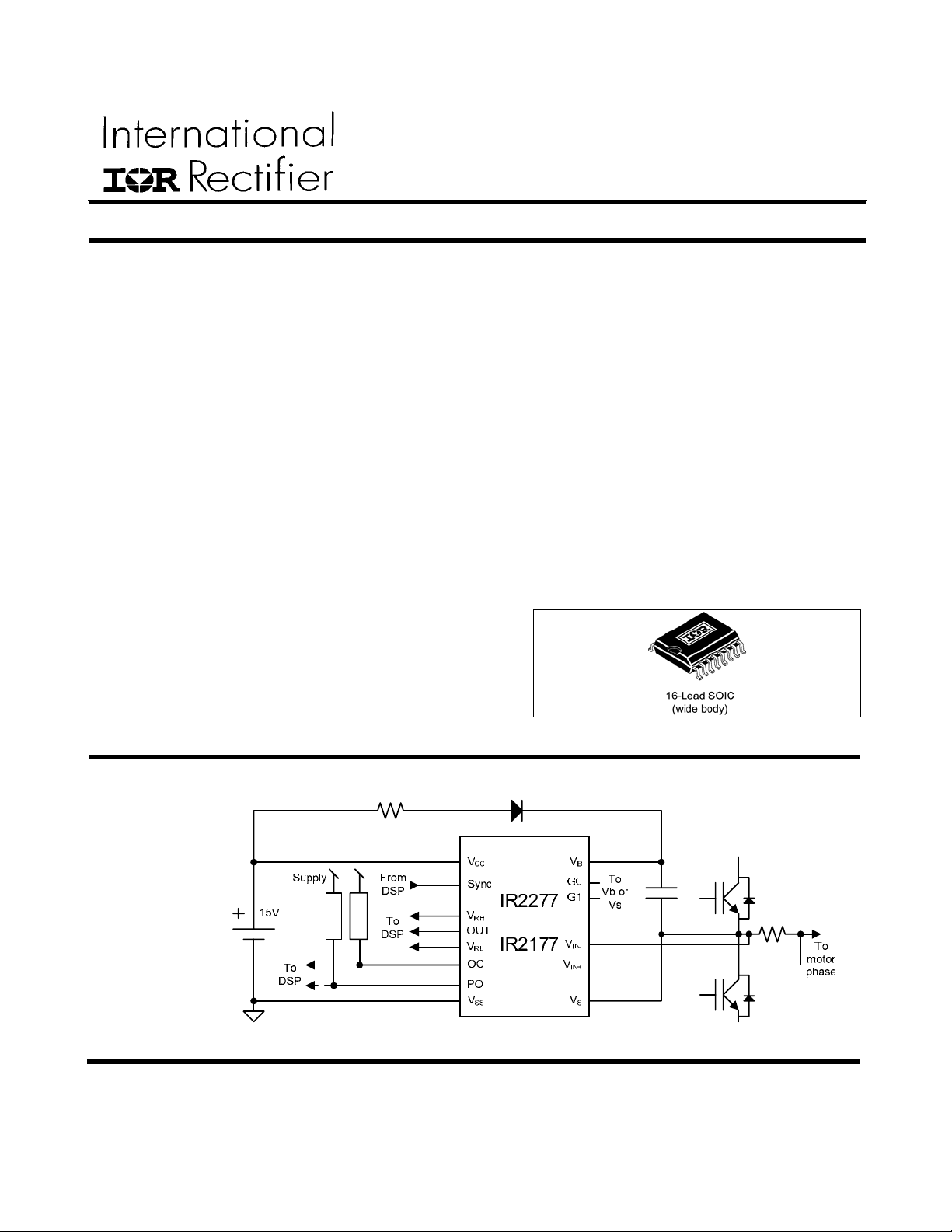
Typical Connection
(Please refer to
Lead Assignments
for correct pin
configuration. This
diagram shows
electrical
connections only)
1 www.irf.com
IR2277S/IR2177S(PbF)
Absolute Maximum Ratings
Absolute Maximum Ratings indicate sustained limits beyond which damage to the device may occur. All voltage parameters
are absolute voltages referenced to V
Dissipation ratings are measured under board mounted and still air conditions.
, all currents are defined positive into any lead. The Thermal Resistance and Power
SS
Symbol Definition Min. Max. Units
VB High Side Floating Supply Voltage
VS High Side Floating Ground Voltage
V
/ V
in+
High-Side Inputs Voltages
in-
G0 / G1 High-Side Range Selectors
VCC Low-Side Fixed Supply Voltage - 0.3 25 V
Sync Low-Side Input Synchronization Signal
VRH/VRL DSP Reference Hi gh and Low Voltages - 0.3 VCC + 0.3 V
Out Analog Output Voltage - 0.3 VCC + 0.3 V
PO PWM Output - 0.3 VCC + 0.3 V
OC Over Current Output Voltage - 0.3 VCC + 0.3 V
dVS/dt Allowable Offset Voltage Slew Rate 50 V/ns
PD Maximum Power Dissipation 250 mW
R
Thermal Resistance, Junction to Ambient 90 ºC/W
thJA
TJ Junction Temperature -40 125 ºC
TS Storage Temperature -55 150 ºC
TL Lead Temperature (Soldering, 10 seconds) 300 ºC
IR2277 - 0.3 1225
V
V
- 25
B
- 5
S
- 0.3
S
625
+ 0.3 V
V
B
+ 0.3 V
V
B
+ 0.3 V
V
B
IR2177 - 0.3
V
- 0.3 VCC + 0.3 V
V
Recommended Operating Conditions
For proper operation the device should be used within the recommended conditions. All voltage p arameters are absolute
voltages referenced to V
. The
ss
Symbol
VBS High Side Floating Supply Voltage (V
VS
V
/ V
in+
G0 / G1 High-Side Range Selectors Note 1 Note1
VCC Low Side Logic Fixed Supply Voltage 8 20 V
Sync Low-Side Input Synchronization Signal
f
sync
PO PWM Output -0.3 Note 2 V
OC Over Current Output Voltage -0.3 Note 2 V
VRH
VRL
TA
Note 1: Shorted to VS or V
Note 2: Pull-Up Resistor to
High Side Floating Ground Voltage
High-Side Inputs Voltages VS - 5.0 VS + 5.0 V
in-
Sync Input Frequency
OUT Reference High Voltage 3 V
OUT Reference Low Voltage V
Ambient Temperature -40 125 ºC
B
V
CC
offset rating is tested with all supplies biased at 15V differential.
V
s
Definition Min. Max. Units
V
)
V
-
B
S
IR2277 1200
IR2177
Using PO 4 20
Using OUT 8 20
+ 8.0 VS + 20 V
S
VSS V
-5
V
SS
600
V
CC
-2.5 V
CC
-3 V
RH
V
kHz
2 www.irf.com
IR2277S/IR2177S(PbF)
Static Electrical Characteristics
, VBS = 15V unless otherwise specified. Temp=27°C; Vin=V
V
CC
Pin: V
, VSS, VB, VS
CC
Symbol Definition Min. Typ. Max. Units
I
Quiescent VBS supply current 1 2.2 mA
QBS
I
Quiescent VCC supply current 6 mA
QCC
IR2277 50
ILK Offset supply leakage current
IR2177 50
Pin: V
in+
, V
, Sync, G0, G1, OC
in-
Symbol Definition Min. Typ. Max. Units
V
Maximum input voltage before saturation 250 mV
inmax
V
Minimum input voltage before saturation -250 mV
inmin
VIH Sync Input High threshold 2.2 V See Figure 1
VIL Sync Input Low threshold 0.8
Vhy Sync Input Hysteresis 0.2 V See Figure 1
I
V
vinp
Ipu G0, G1 pull-up Current -20 -8 µA
|V
|
octh
R
Sync
R
Over Current On Resistance 25 75
onOC
input current -18 -6 µA
in+
Over Current Activation Threshold 300 470 mV
SYNC to VSS internal pull-down 6 12
- Vin.
in+
µA
V
kΩ
Ω
Test
Conditions
f
= 10kHz,
sync
20kHz
f
= 10kHz,
sync
20kHz
V
= VS =
B
1200V
= VS = 600V
V
B
Test
Conditions
See Figure 1
f
= 4kHz to
sync
20kHz
G1, G0 = V
5V
@ I = 2mA
Figure
See
B
3
-
Schm itt trig g e r
SYNC
R
sync
V
IL
V
hy
V
IH
V
SS
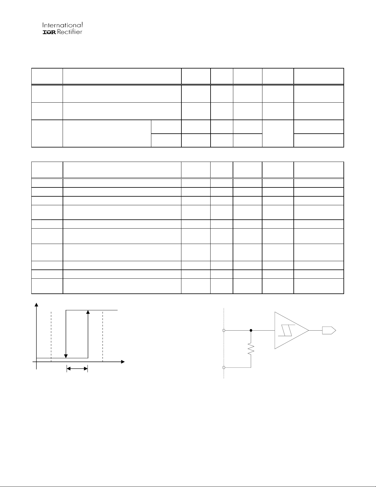
Figure 1: Sync input thresholds Figure 2: Sync input circuit
IR2277S/IR2177S(PbF)
j
Pin: PO
Symbol Definition Min. Typ. Max. Units
V
POs
∆V
POs
∆T
∆V
POs
Gp PWM Output Gain -38 -40.5 -42.5 %/V Vin=±250mV
∆G
/
p
CMRR
PO
V
POlin
∆ V
lin
V
thPO
PSRR PO PSRR for PO Output 0.2 %/V
R
onPO
Note1: Refer to PO output description for channels definition
Input offset voltage measured by PWM
output
/
Input offset voltage temperature drift TBD
-50 20 mV
µV/°C
∆offset between samples on channel1
and channel2 measured at PO (See
-10 10 mV
Note1)
∆Tj
PWM Output Gain Temperature Drift TBD %/(V
PO Output common mode (V
) rejection 0.2 m%/V
S
ºC)
*
PO Linearity 0.07 0.2 % 10kHz
∆Tj
PO Linearity Temperature Drift TBD %/ºC 10kHz
/
PO threshold for OC reset 0.8 1.6 V
PO On Resistance 25 75
Ω
Test
Conditions
R
=500 Ω
pull-up
= 4, 20kHz
f
sync
V
Ext supply=5V
(See Figure 6)
OC active (See
V
=2.75V
threshold
f
= 10kHz
sync
See Figure 6
= 0,
V
s-Vss
600V
f
= 10kHz
sync
Figure 4
CC=VBS
)
=
8,20V
@ I = 2mA
See Figure 3
PO
or
OC
R
ON
V
SS
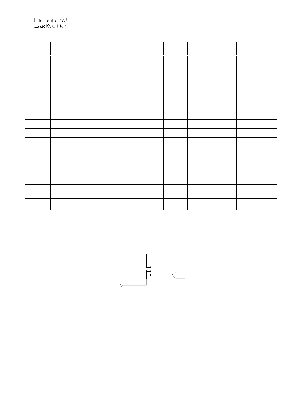
Figure 3: PO and OC open collector circuit
4 www.irf.com
Internal signal
IR2277S/IR2177S(PbF)
Pin: OUT, VRH, VRL
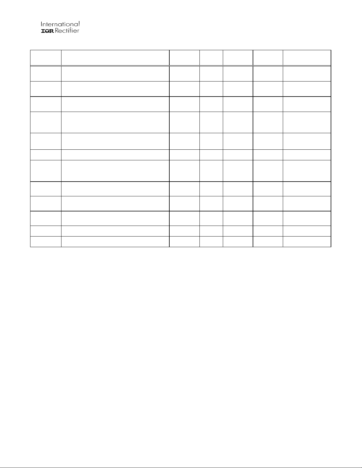
Symbol Definition Min. Typ. Max. Units
R
V
REF
V
aos
∆ V
/
aos
∆Tj
∆V
aos
to VRL input resistance 36 84
RH
Input offset voltage measured by
analog output
-100 50 mV
kΩ
Input offset voltage temperature drift TBD µV / ºC
∆offset between samples on channel1
and channel2 measured at OUT
(Note1)
Test
Conditions
f
= 8kHz, 20
sync
kHz
Measured by
analog output
f
= 8kHz, 20
sync
kHz
Ga Analog Output Gain -20% 2VR +20% V/V
-1
∆Ga / ∆Tj
CMRR
OUT
V
OUTlin
∆ V
/
lin
∆Tj
PSRR
OUT
V
Vout Low Saturation 0 50 mV Vin= -500mV
OUTl
V
OUTh
Note1: Refer to PO output description for channels definition
Analog Output Gain Temperature Drift TBD ºC
Analog Output common mode (VS
offset) rejection
100 dB
Out Linearity 0.3 0.7 %
Out Linearity Temperature Drift TBD %/ºC
PSRR for Analog Output 30 100 dB
Vout High Saturation VRH+0.2 VRH+0.7 V Vin = +500mV
VR=VRH-VRL=3V
Vs-Vss=0V,
f
sync
f
sync
f
sync
V
CC
600V
= 10kHz
= 8kHz,
20kHz
= 8kHz,
20kHz
= VBS =8V,
20V
5 www.irf.com
IR2277S/IR2177S(PbF)
AC Electrical Characteristics
V
V
BIAS
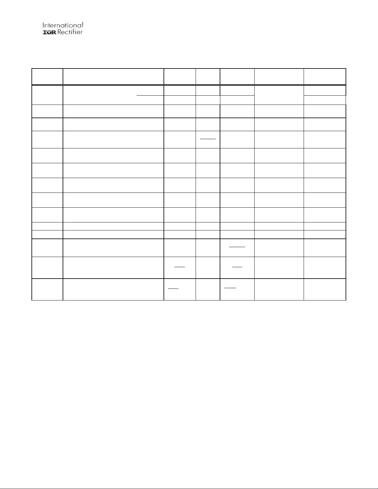
Symbol Definition Min. Typ. Max. Units
f
sync
f
out
BW Bandwidth (@ -3 dB)
GD Group Delay (input filter)
, VBS) = 15V unless otherwise specified. Temp=27°C.
(
CC
PWM frequency
PO 4
OUT 8
Throughput
Test
Conditions
f2⋅
sync
f
sync
1
f4
⋅
sync
20
kHz
20
ksample/sec
kHz
µs
D
min
D
max
t
dOCon
T
OCoff
C
Analog output load capacitor 0 50 nF NOTE 2
load
SL
OUT
t
Output settling time (1%) 5 30 µs
settl
MD Measure Delay
SR
SR
OUT
Note 1: negative logic, see Figure 4 on page 7
Note 2: Cload < 5 nF avoids overshoot
Minimum Duty Cycle (Note 1) 10 % Vin=+V
Maximum Duty Cycle (Note 1) 30 % Vin=-V
De-bounce time of OC 2.7 3.5 4.7 µs See Figure 4
Time to reset OC forcing PO 0.5 µs
Analog output (OUT) Slew Rate 0.2 1 V/µs
Step response (max time to reach
steady state) for PO output
Step response (max time to reach
steady state) for OUT output
30.0
f2
⋅
sync
51.0
f
sync
51.0
t+
settl
f
sync
3.1
f
sync
3.1
t+
sync
settl
f
µs
µs
µs
See
See
Figure 5
See
Figure 5
C
out
C
out
inmax
inmin
Figure
≤ 5 nF
≤ 5 nF
4
6 www.irf.com
 Loading...