Data Sheet No. PD60234 revB
IR22771S/IR21771S(PbF)
Phase Current Sensor IC for AC motor control
Features
• Floating channel up to 600V for IR21771 and 1200V for
IR22771
• Synchronous sampling measurement system
• High PWM noise (ripple) rejection capability
• Digital PWM output
• Fast Over Current detection
• Suitable for bootstrap power supplies
• Low sensing latency (<7.5 µsec @20kHz)
Description
IR21771/IR22771 is a high voltage, high speed, single phase
current sensor interface for AC motor drive applications. The
current is sensed by an external shunt resistor. The IC converts the
analog voltage into a time interval through a precise circuit that also
performs a very good ripple rejection showing small group delay.
The time interval is level shifted and given to the output. The ma x
throughput is 40 ksample/sec suitable for up to 20 kHz
asymmetrical PWM modulation and max delay is <7.5
(@20kHz). Also a fast over current signal is provided for IGBT
protection.
µsec
Product Summary
V
(max) IR22771 1200 V
OFFSET
IR21771 600V
V
range ±250mV
in
Bootstrap supply range 8-20 V
Floating channel quiescent
current (max)
Sensing latency (max) 7.5 µsec
Throughput 40ksample/sec
Over Current threshold (max) ±470 mV
2.2 mA
(@20kHz)
(@20kHz)
Package
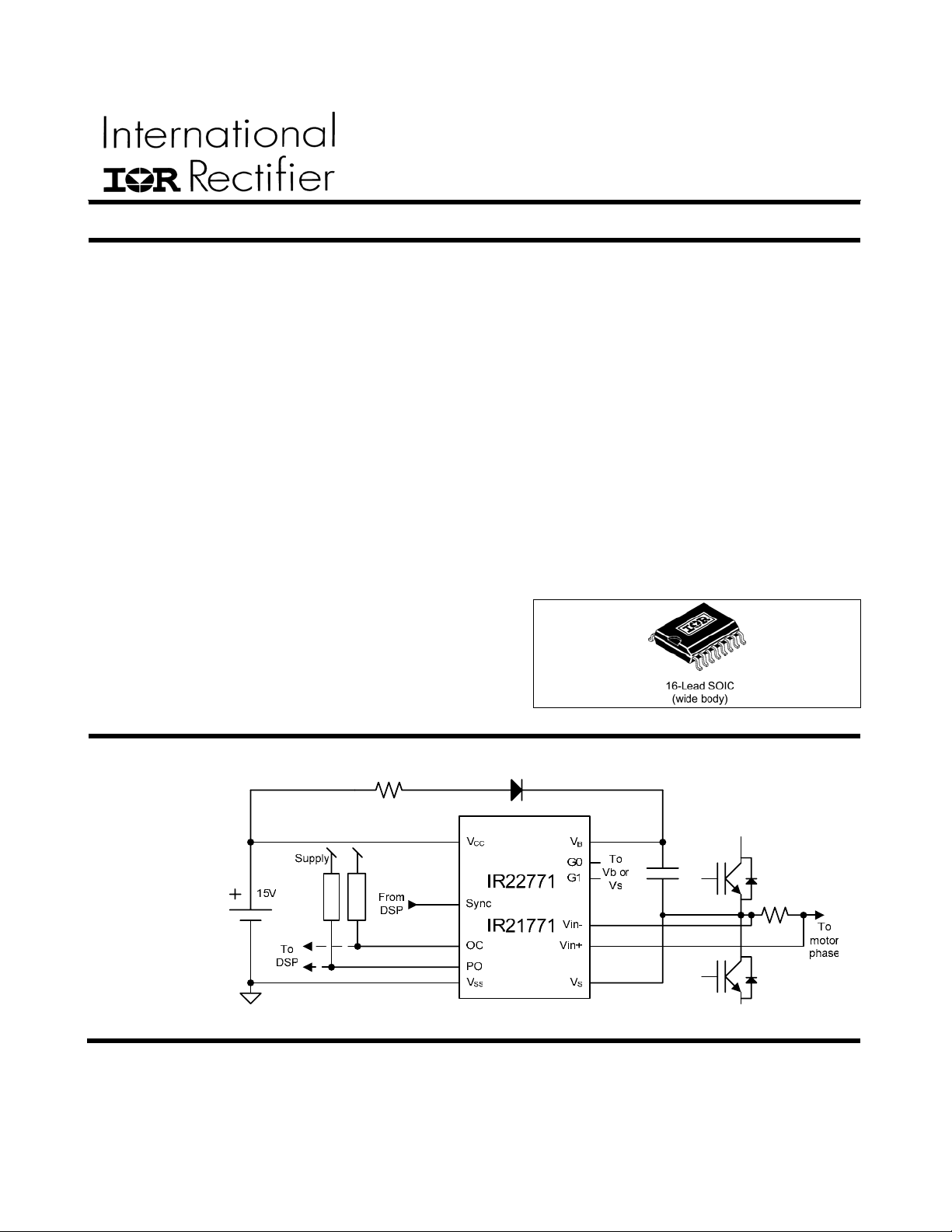
Typical Connection
(Please refer to
Lead Assignments
for correct pin
configuration. This
diagram shows
electrical
connections only)
1 www.irf.com
IR22771S/IR21771S(PbF)
Absolute Maximum Ratings
Absolute Maximum Ratings indicate sustained limits beyond which damage to the device may occur. All voltage parameters
are absolute voltages referenced to V
Dissipation ratings are measured under board mounted and still air conditions.
Symbol Definition Min. Max. Units
VB High Side Floating Supply Voltage
VS High Side Floating Ground Voltage
V
/ V
High-Side Inputs Voltages
in+
in-
G0 / G1 High-Side Range Selectors
VCC Low-Side Fixed Supply Voltage - 0.3 25 V
Sync Low-Side Input Synchronization Signal
PO PWM Output - 0.3 VCC + 0.3 V
OC Over Current Output Voltage - 0.3 VCC + 0.3 V
dVS/dt Allowable Offset Voltage Slew Rate 50 V/ns
PD Maximum Power Dissipation 250 mW
R
Thermal Resistance, Junction to Ambient 90 ºC/W
thJA
TJ Junction Temperature -40 125 ºC
TS Storage Temperature -55 150 ºC
TL Lead Temperature (Soldering, 10 seconds) 300 ºC
Recommended Operating Conditions
For proper operation the device should be used within the recommended conditions. All voltage p arameters are absolute
voltages referenced to
Symbol
VBS High Side Floating Supply Voltage (V
VS
V
/ V
in+
G0 / G1 High-Side Range Selectors Note 1 Note1
VCC Low Side Logic Fixed Supply Voltage 8 20 V
Sync Low-Side Input Synchronization Signal
f
Sync Input Frequency 4 20 kHz
sync
PO PWM Output -0.3 Note 2 V
OC Over Current Output Voltage -0.3 Note 2 V
TA
Note 1: Shorted to VS or V
Note 2: Pull-Up Resistor to V
High Side Floating Ground Voltage
High-Side Inp uts Voltages VS - 5.0 VS + 5.0 V
in-
Ambient Temperature -40 125 ºC
. The
V
SS
B
CC
; all currents are defined positive into any lead. The Thermal Resistance and Power
SS
IR22771 - 0.3 1225 V
V
V
V
B
- 25
B
- 5
B
- 0.3
625 V
+ 0.3 V
V
B
+ 0.3 V
V
B
+ 0.3 V
V
B
- 0.3 VCC + 0.3 V
IR21771 - 0.3
offset rating is tested with all supplies biased at 15V differential.
V
S
Definition Min. Max. Units
V
)
V
-
B
S
IR22771 -5
IR21771 -5 600 V
+ 8.0 VS + 20 V
S
V
SS
1200 V
V
V
CC
2 www.irf.com
IR22771S/IR21771S(PbF)
Static Electrical Characteristics
VCC, VBS = 15V unless otherwise specified. Temp=27°C; Vin=V
Pin: VCC, VSS, VB, VS
Symbol Definition Min Typ Max Units
I
Quiescent VBS supply current 1 2.2 mA
QBS
I
Quiescent VCC supply current 6 mA
QCC
ILK
Offset supply leakage
current
Pin: V
in+
, V
, Sync, G0, G1, OC
in-
Symbol Definition Min Typ Max Units
V
Maximum input voltage before saturation 250 mV
inmax
V
Minimum input voltage before saturation -250 mV
inmin
VIH Sync Input High threshold 2.2 V See Figure 1
VIL Sync Input Low threshold 0.8
Vhy Sync Input Hysteresis 0.2 V See Figure 1
I
V
vinp
Ipu G0, G1 pull-up Current -20 -8 µA
|V
|
octh
R
Sync
R
Over Current On Resistance 25 75
onOC
input current -18 -6 µA
in+
Over Current Activation Threshold 300 470 mV
SYNC to VSS internal pull-down 6 12
IR22771 50 µA
IR21771 50 µA V
- Vin.
in+
V
kΩ
Ω
Test
Conditions
f
= 10kHz,
sync
20kHz
f
= 10kHz,
sync
20kHz
V
= VS =
B
1200V
= VS = 600V
B
Test
Conditions
See Figure 1
f
= 4kHz to
sync
20kHz
G1, G0 = V
5V
@ I = 2mA
Figure
See
B
3
-
Schmitt trigg e r
SYNC
R
sync
V
SS
V
IL
V
hy
V
IH
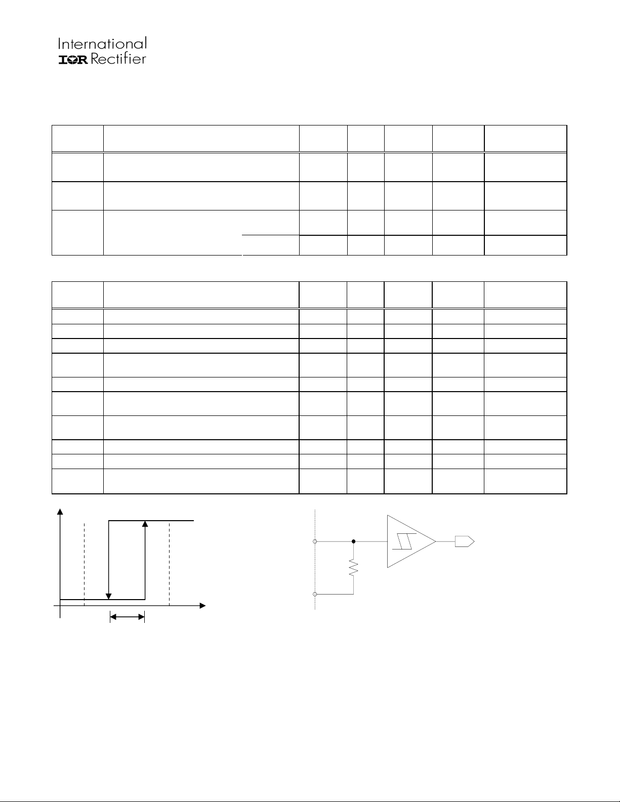
Figure 1: Sync input thresholds Figure 2: Sync input circuit
3 www.irf.com
IR22771S/IR21771S(PbF)
j
Pin: PO
Symbol Definition Min Typ Max Units
V
POs
Test
Conditions
R
=500 Ω
pull-up
= 4, 20kHz
f
Input offset voltage measured by PWM
output
-50 20 mV
sync
V
threshold
=2.75V
Ext supply=5V
(See Figure 6)
∆V
/
∆T
∆V
POs
Pos
Input offset voltage temperature drift TBD
∆offset between samples on channel1
and channel2 measured at PO (See
-10 10 mV
Note1)
µV/°C
f
= 10kHz
sync
See Figure 6
Gp PWM Output Gain -38 -40.5 -42.5 %/V Vin=±250mV
∆G
∆Tj
/
p
CMRR
PO
V
PO Linearity 0.07 0.2 % f
Polin
∆ V
lin
V
PO threshold for OC reset 0.8 1.6 V
thPO
PWM Output Gain Temperature Drift TBD %/(V
PO Output common mode (V
∆Tj
PO Linearity Temperature Drift TBD %/ºC f
/
) rejection 0.2 m%/V
S
PSRR PO PSRR for PO Output 0.2 %/V
R
PO On Resistance 25 75
onPO
Note1: Refer to PO output description for channels definition
ºC)
*
S-VSS
= 0,
V
600V
f
= 10kHz
sync
= 10kHz
sync
= 10kHz
sync
OC active (See
Figure 4
V
CC=VBS
)
=
8,20V
Ω
@ I = 2mA
See Figure 3
PO
or
OC
R
ON
V
SS
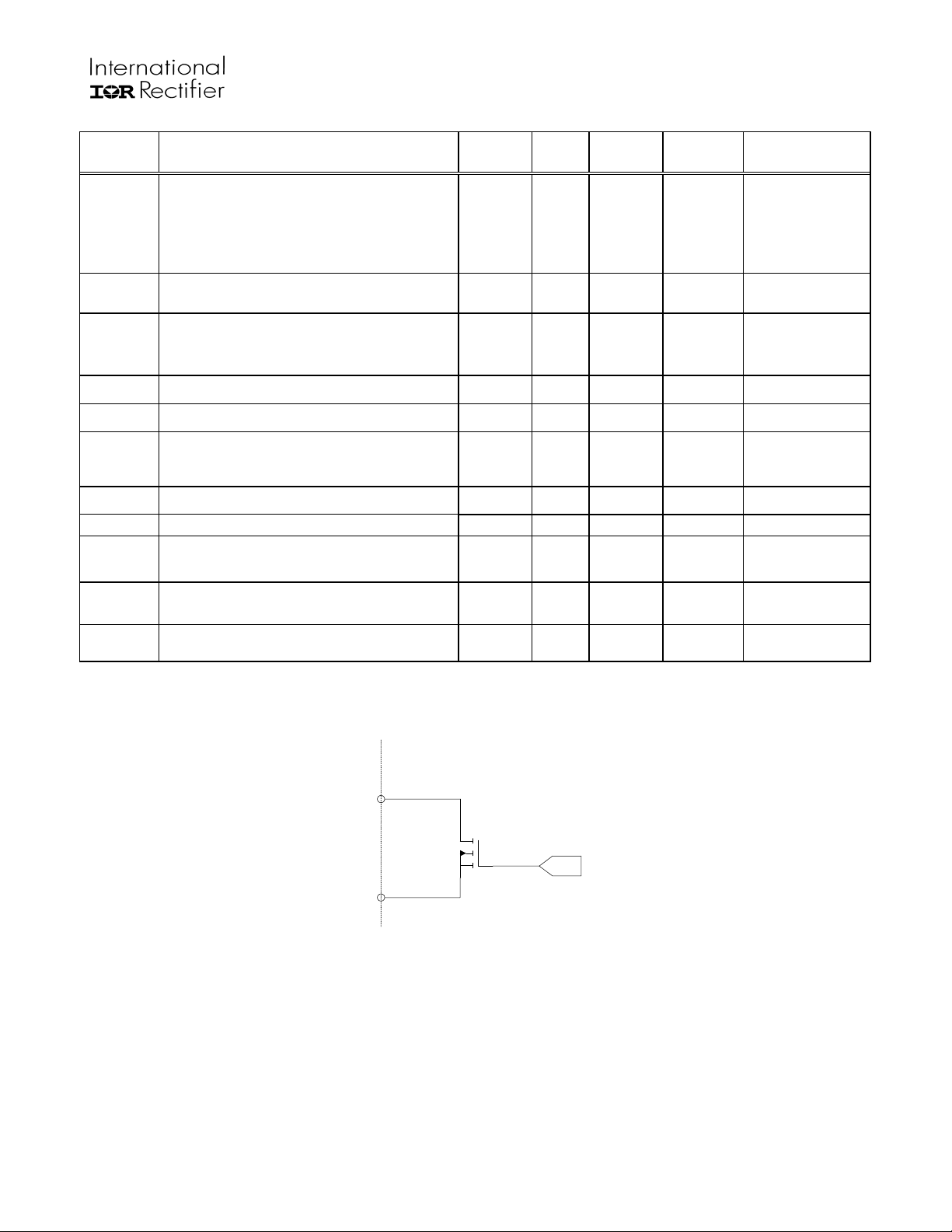
Figure 3: PO and OC open collector circuit
Internal signal
4 www.irf.com
IR22771S/IR21771S(PbF)
⋅
AC Electrical Characteristics
V
V
BIAS
Symbol Definition Min Typ Max Units
f
sync
f
out
BW Bandwidth (@ -3 dB)
GD Group Delay (input filter)
, VBS) = 15V unless otherwise specified. Temp=27°C.
(
CC
PWM frequency 4
Throughput
fsync2
fsync
1
fsync4
⋅
Conditions
20 kHz
ksample/sec
kHz
µs
Test
D
min
D
max
t
dOCon
T
OCoff
Minimum Duty Cycle (Note 1) 10 % Vin=+V
Maximum Duty Cycle (Note 1) 30 % Vin=-V
De-bounce time of OC 2.7 3.5 4.7 µs See Figure 4
Time to reset OC forcing PO 0.5 µs
MD Measure Delay
SR
Note 1: negative logic, see fig. 4 on page 7
Note 2: Cload < 5 nF avoids overshoot
Step response (max time to reach
steady state)
51.0
fsync
30.0
fsync2
⋅
3.1
fsync
inmax
inmin
Figure
See
4
µs
µs See Figure 5
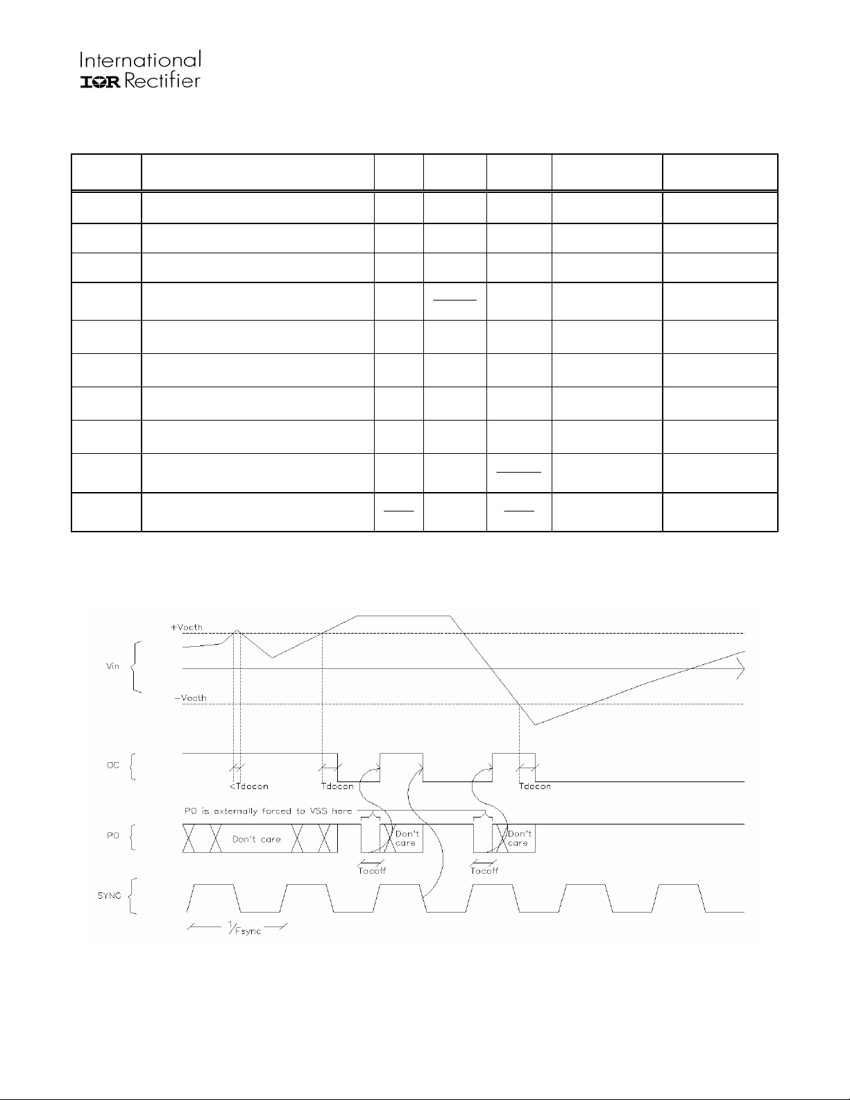
Figure 4: OC timing diagram
5 www.irf.com
 Loading...