Data Sheet No. PD60219 rev.B
IR2161(S) & (PbF)
HALOGEN CONVERTOR CONTROL IC
Features
Intelligent half-bridge driver
•
Auto Resetting Short Circuit Protection
•
Auto Resetting Overload Protection
•
Packages
• Externally Triggerable Latching Shutdown
• Latching Overtemperature Protection
• Frequency Modulation “dither” (for lower EMI)
• Micropower Startup (<300 µA)
• Phase Cut dimmable for leading / trailing edge
• Output Voltage Shift Compensation.
8-Lead PDIP
IR2161
8-Lead SOIC
IR2161S
• Real Softstart
• Adaptive Dead Time
• Small 8 Pin DIP/SOIC Package
• Also available LEAD-FREE (PbF)
Description
The IR2161 is a dedicated Intelligent Half bridge Driver IC for a Halogen convertor (electronic transformer). It
includes all necessary protection features and also allows the Convertor to be dimmed externally with a
standard phase cut dimmer with both leading or trailing edge types. This IC provides the advantage of reduced
thermal stress in the lamp due to softstart. There is also compensation of the output voltage for load regulation.
It enables the convertor to operate with extremely low harmonic distortion over the full range of loads. The
IR2161 includes adaptive deadtime to allow cool running MOSFETs and improves the EMI behaviour due to
frequency modulation (dither). All the features are integrated in a small 8 pin DIP/SOIC package to allow for a
size reduction in the next generation of convertors.
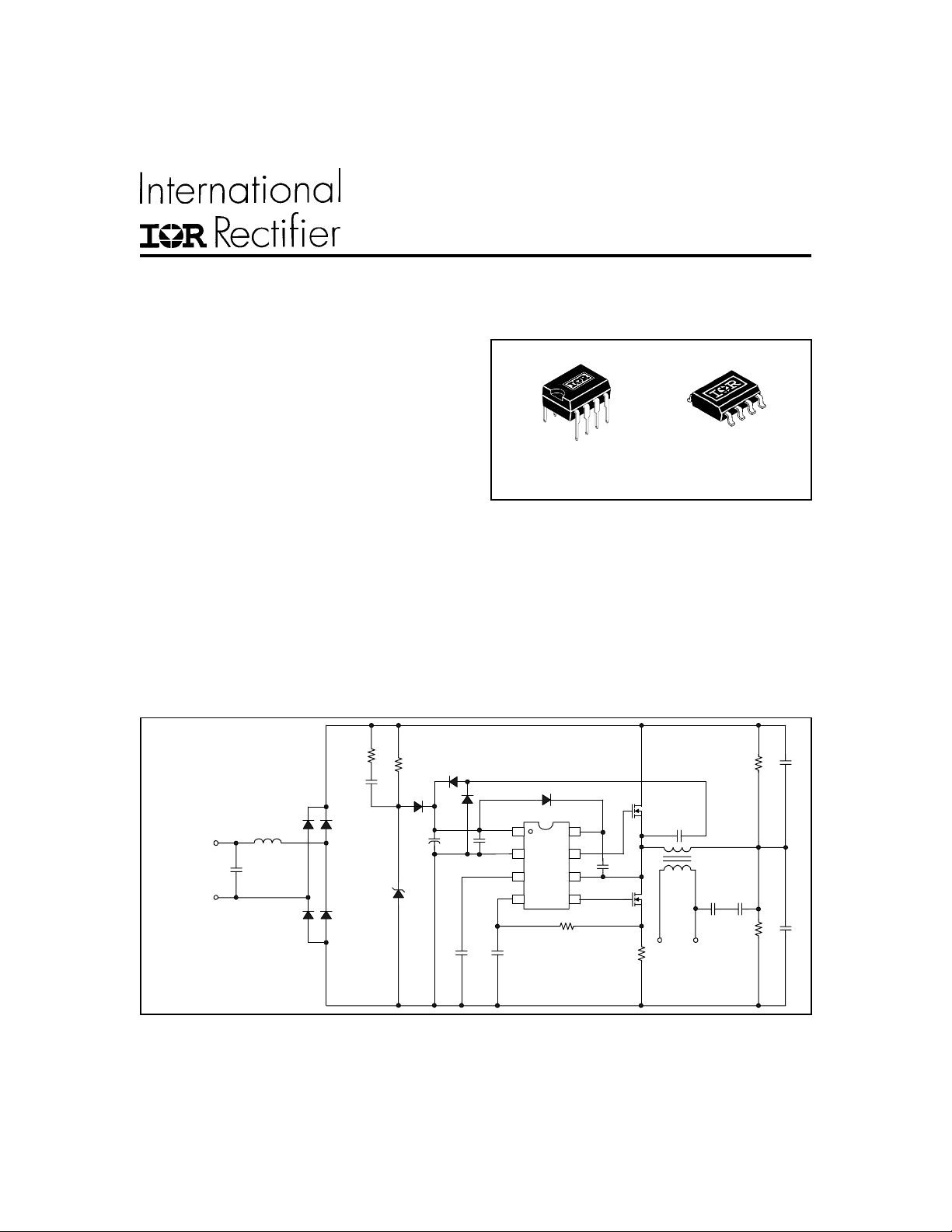
Typical Connections
AC LINE
INPUT
CLF
LF
D1 D2
D3 D4
RD
CD
RS
DCP1
CS
1
2
3
4
CCS
DB
8
IR2161
7
6
5
RL
Q1
Q2
OUTPUT
CSNUB
12VAC
VB
HO
CB
VS
LO
RCS
CVCC2
DCP2
VCC
COM
CSD
CSD
DS
CVCC1
VZ
R1
T1
C3 C4
R2 C2
C1
Note: Throughout this data sheet “convertor” is spelled in accordance with standard IEC 61047 “DC or AC supplied convertors
for filament lamps – Performance requirements”.
www.irf.com 1
IR2161(S) & (PbF)
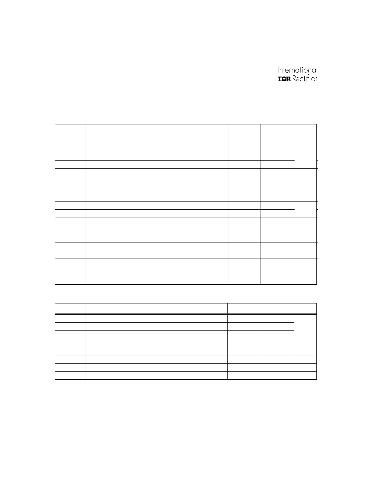
Absolute Maximum Ratings
Absolute maximum ratings indicate sustained limits beyond which damage to the device may occur. All voltage parameters
are absolute voltages referenced to COM, all currents are defined positive into any lead. The thermal resistance and power
dissipation ratings are measured under board mounted and still air conditions.
Symbol Definition Min. Max. Units
V
B
V
S
V
HO
V
LO
IO
MAX
V
CSDMAX
V
CS
I
CS
I
CC
dV/dt Allowable offset voltage slew rate -50 50 V/ns
P
D
Rth
JA
T
J
T
S
T
L
High side floating supply voltage -0.3 625
High side floating supply offset voltage VB - 25 VB + 0.3
High side floating output voltage VS - 0.3 V
B
+ 0.3
Low side output voltage -0.3 VCC + 0.3
Maximum allowable output current (HO,LO) due to external -500 500
power transistor miller effect
CSD pin voltage -0.3 V
Current sense pin voltage -0.3 V
CC
CC
+ 0.3
+ 0.3
Current sense pin current -5 5
Supply current (Note 1) -20 20
Maximum power dissipation @ T
PD = (T
JMAX-TA
)/Rth
(8 Lead SOIC) — 0.625
JA
≤ +25°C (8 Lead DIP) — 1
A
Thermal resistance, junction to ambient (8 Lead DIP) — 125
(8 Lead SOIC) — 200
Junction temperature -55 150
Storage temperature -55 150
Lead temperature (soldering, 10 seconds) — 300
V
mA
V
mA
W
°C/W
°C
Recommended Operating Conditions
For proper operation the device should be used within the recommended conditions.
Symbol Definition Min. Max. Units
V
BS
V
BSMIN
V
S
V
CC
I
CC
C
SD
I
CS
T
J
Note 1: This IC contains a zener clamp structure between the chip VCC and COM which has a nominal breakdown
Note 2: Enough current should be supplied into the VCC pin to keep the internal 15.6V zener clamp diode on this pin
2 www.irf.com
High side floating supply voltage VCC - 0.7 V
CLAMP
Minimum required VBS voltage for proper HO functionality 4.3 —
Steady state high-side floating supply offset voltage -1 600
Supply voltage V
CCUV+
V
CLAMP
V
Supply current (Note 2) 10 mA
CSD pin external capacitor 47 — nF
Current sense pin current -1 1 mA
Junction temperature -25 125 °C
voltage of 15.6V. Please note that this supply pin should not be driven by a DC, low impedance power source
greater than the V
regulating its voltage, V
specified in the Electrical Characteristics section.
CLAMP
.
CLAMP
IR2161(S) & (PbF)
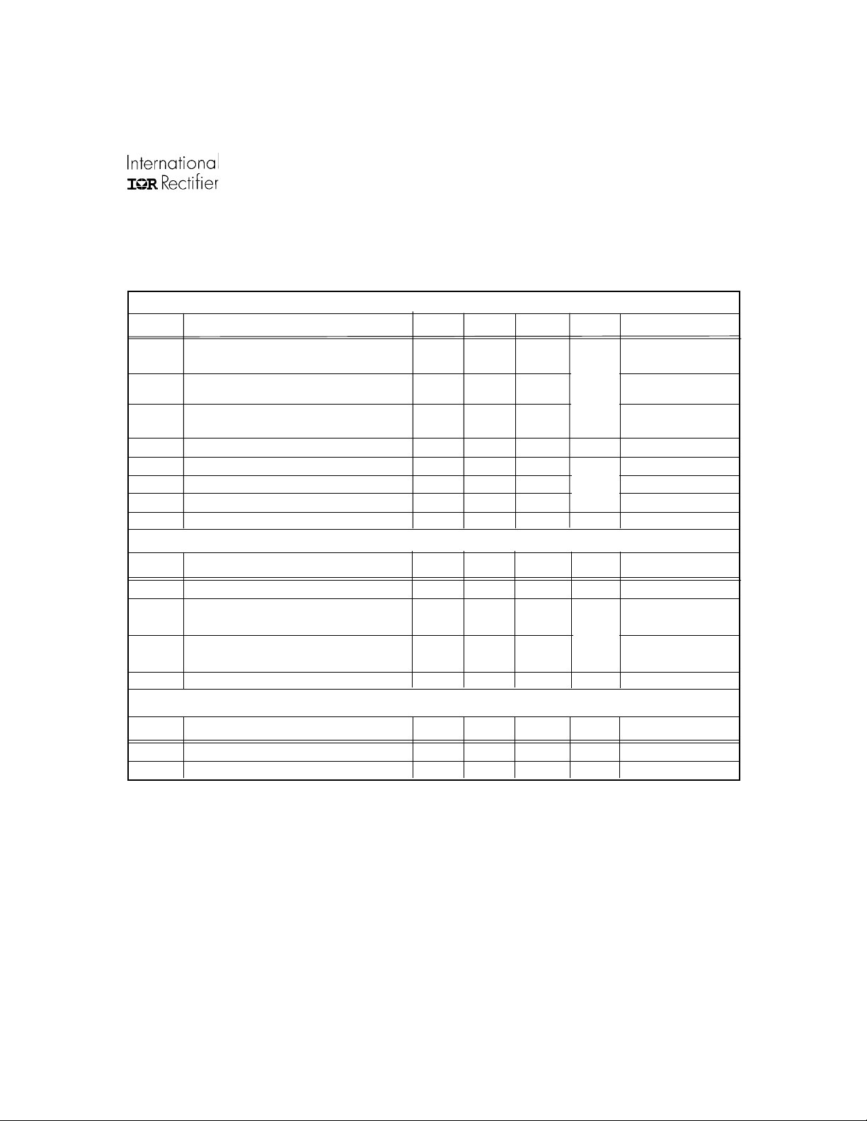
Electrical Characteristics
VCC = VBS = V
Supply Characteristics
Symbol Definition Min. Typ. Max. Units Test Conditions
V
CCUV+VCC
V
CCUV-
V
CCUVL-VCC
I
QCCUV
I
CCFLT
I
VCC current (low frequency) — 2.0 3.0 VCC=14V,VCSD=5.2V
CC
LF
I
VCC current (high frequency) — 4.0 7.0 VCC=14V,VCSD=0V
CC
HF
V
CLAMPVCC
Floating Supply Characteristics
Symbol Definition Min. Typ. Max. Units Test Conditions
V
BSM IN
I
BSHF
I
BSLF VBS
I
LEAK
= 14V, +/- 0.25V, VCSD = 5.0V, C
BIAS
supply undervoltage positive going
threshold 11.5 12.1 12.7 VCC rising from 0V
VCC supply undervoltage negative going
threshold 10 10.5 11 VCC falling from 14V
supply softstart reset negative going
threshold — — 5.5 VCC - V
UVLO mode quiescent current — 250 300 VCC = 11V
Fault-mode quiescent current — 1.4 2.0 CS=8V, VCSD=0V
zener clamp voltage 14.5 15.4 16.5 V ICC = 5mA
Minimum V
V
high frequency supply current — 3.0 — VCC=14V,VBS=14V,
BS
low frequency supply current — 0.8 — VCC=14V,VBS=14V,
Offset supply leakage current — — 50 µAV
to start oscillation at HO 3.0 3.6 4.3 V
BS
LO =CHO
= 1000 pF, and TA = 25°C unless otherwise specified.
V
(-2V)
µA
mA
mA
CCUV-
VCSD=0V
VCSD=5.2V
= VS = 600V
B
Voltage Compensation Characteristics (Run Mode)
Symbol Definition Min. Typ. Max. Units Test Conditions
V
CSD (min)
V
CSD (max)
www.irf.com 3
Min CSD voltage (in Run Mode) — 0 — V VCS = 0V
Max CSD voltage (in Run Mode) — 5.5 — V VCS = 0.4V
IR2161(S) & (PbF)
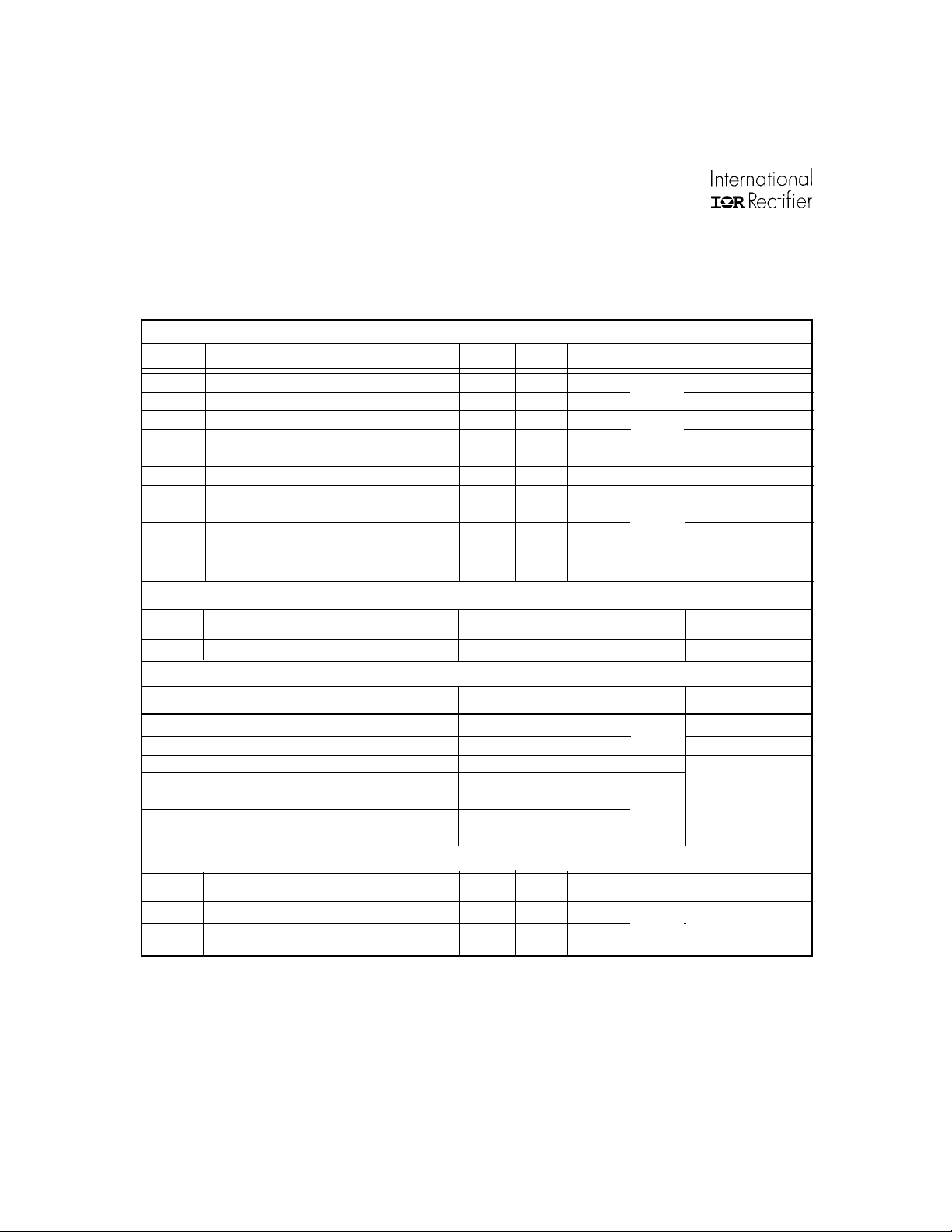
Electrical Characteristics (cont’d)
VCC = VBS = V
Shutdown Circuit Characteristics
Symbol Definition Min. Typ. Max. Units Test Conditions
V
CSOL
V
CSSC
I
OL
I
SC
I
RESET
V
CSLATCH
T
CSLATCH
V
CSDOL
V
CSDSD
V
CSDRS
Thermal Shutdown Characteristics
Symbol Definition Min. Typ. Max. Units Test Conditions
T
SD
Oscillator Characteristics
= 14V, +/- 0.25V, VCSD = 5.0V, C
BIAS
Overload threshold (CS PID) 0.47 0.56 0.64
CSD short circuit threshold (CS PID) 1 1.2 1.4
CSD overload charging current
CSD short circuit charging current 75 100 120 VCS=1.5V,VCSD=7V
CSD shutdown reset current 0.1 0.7
Latched shutdown threshold
Latched shutdown delay 1 µsec VCS>VCSLATCH
Begin fault timing
Positive going threshold for oscillator
shutdown
Negative going threshold for oscillator restart
Latched over temperature limit
LO =CHO
= 1000 pF, and TA = 25°C unless otherwise specified.
V
6
—
—
—
—
—
9 12 VCS=0.8V,VCSD=7V
uA
9
5
12
2.4
135
—
—
—
—
—
—
oC
VCSD=14V
V
VCS>VCSOL
VCS > VCSOL
V
Symbol Definition Min. Typ. Max. Units Test Conditions
f
(min)
f
(max)
D Oscillator duty cycle
LO(max)
DT
DT
HO(max)
Minimum oscillator frequency — 34 — VCSD = 5.3V
Maximum oscillator frequency in RUN mode
Maximum LO output deadtime — 1.0 —
(run mode default)
Maximum HO output deadtime — 1.0 —
(run mode default)
—
70
— 50 — %
—
kHz
µsec
VCSD = 0V
no reset from ADT
Adaptive Dead-Time System Characteristics
Symbol Definition Min. Typ. Max. Units Test Conditions
DT
DT
LO(min)
HO(min)
Minimum LO output deadtime — 700 —
Minimum HO output deadtime — 700
—
4 www.irf.com
Minimum propagation
nsec
delay from ADT to
output drivers
IR2161(S) & (PbF)
Electrical Characteristics (cont.)
VCC = VBS = V
Soft Start Characteristics
Symbol Definition Min. Typ. Max. Units Test Conditions
I
SS
f
SS
Gate Driver Output Characteristics
Symbol Definition Min. Typ. Max. Units Test Conditions
V
V
V
V
t
RISE
t
FALL
IO+ HO, LO source current — 200 —
IO- HO, LO sink current — 300 —
LO voltage when LO is low — COM —
LO=LOW
HO=LOW
LO voltage when LO is high — VCC —
LO=HIGH
HO voltage when HO is high — VCC —
HO=HIGH
Turn-off fall time — 60 140
= 14V, +/- 0.25V, VCSD = 5.0V, C
BIAS
Soft start CSD charge current — 0.5 — mA
Soft start frequency
HO voltage when HO is low — COM —
Turn-on rise time — 110 250
LO =CHO
= 1000 pF, and TA = 25°C unless otherwise specified.
—
115
—
kHz VCC>VCCUV+
CHO=CLO=1nFns
mA
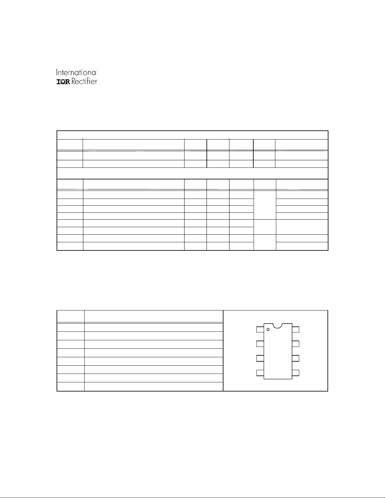
Lead Definitions
Lead Assignments
Symbol Description
V
CC
COM IC power and signal ground
CSD Shutdown timing and compensation capacitor
CS Current sensing input
LO Low-side gate driver output
V
S
HO High side gate driver output
V
B
* Recommended value for CSD is 100nF (all performance data relates to this value)
NOTE: The recommended value for RL is 1K Ohm and CCS is 1nF.
www.irf.com 5
Supply voltage
High-side floating return
High side gate driver floating supply
VCC
COM
CSD
CS
1
IR2161
2
3
4
8
VB
HO
7
6
VS
5
LO
IR2161(S) & (PbF)
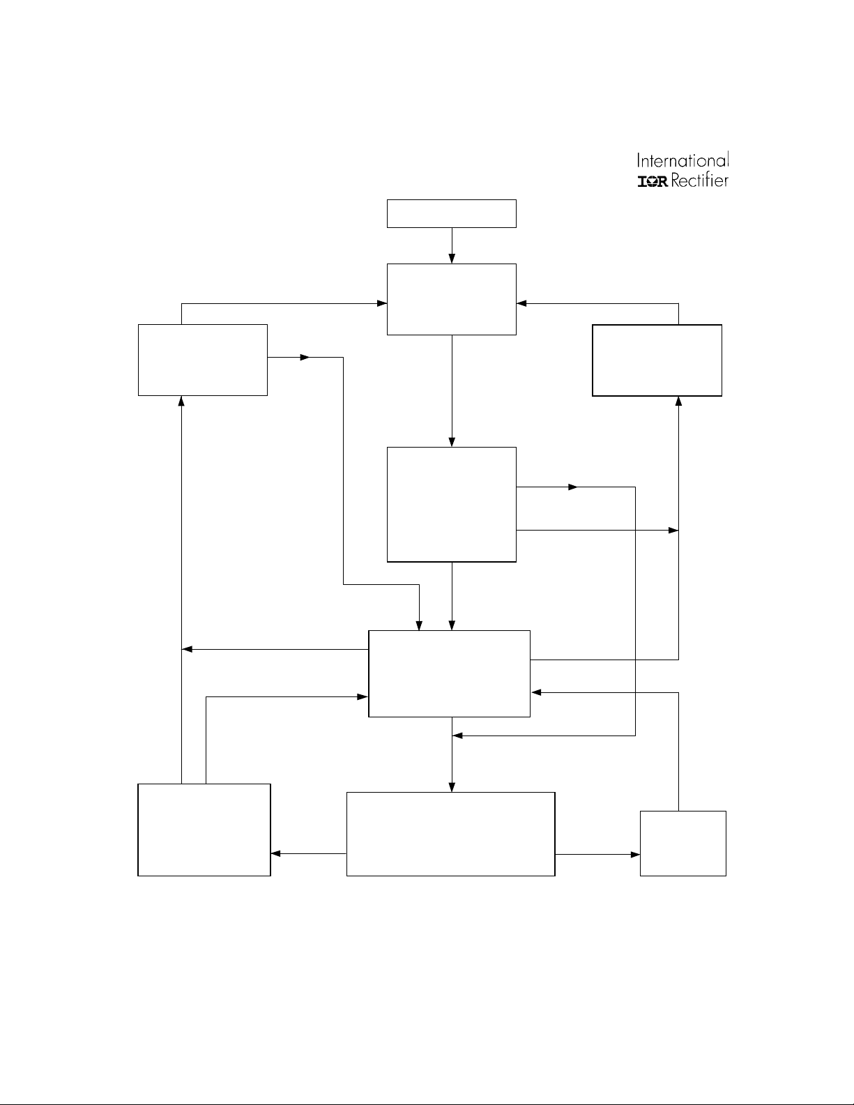
Power Turned On
VCC < 5.5V (V
(Power Turned Off)
STANDBY Mode
1
/
-Bridge Off
2
≅
I
QCC
Oscillator Off
µ
A
300
VCC < 10.5V (V )
(Phase Cut Dimming)
VCC < 10.5V (V )
(Phase Cut Dimming)
Auto-Restart Timeout
(V
< 2.4V) (V
CSD
CSD switched to run mode
CCUVL-
VCC > 12.1V(V
T
<135 C
J
Oscillator On
CCUV-
CCUV-
)
CSDRS
)
CCUV+
jmax
)
)
o
(T
UVLO Mode
1
-Bridge Off
/
2
≅
I
QCC
Oscillator Off
CSD = 0V
300
A
µ
VCC > 12.1V
T
<135 C
J
o
(V
CCUV+
(T
)
jmax
VCC < 5.5V (V
(Power Turned Off)
)
CCUVL-
)
FAULT Mode
1
/
-Bridge Off
2
Oscillator Off
Oscillator On
SOFTSTART
Mode
1
/
- Bridge On
2
Initial frequency 130kHz
CSD charged from Isource
Fault Detected
CS
(Vpk at V
T
<135 C
J
> 0.56V)(V )
o
(T
)
jmax
(Over-Temperature)
CSOL
Frequency ramps down to
f(min)
CSD
V
> 5.2V
(End of SOFTSTART Mode)
CSD switched to Comp function
Fault Detected
CS
(V
<135 C
J
CSLATCH
o
> 9V)
)
(T
jmax
)
RUN Mode
Voltage compensation active
CSD varies between
VCSD (min)
to V
CSD(max)
= 0 for f
= 5.5V for f
(min)
(Vpk at V
T
(Over-Temperature)
CSD switched to
run mode
(max)
SHUTDOWN Mode
1
/
-Bridge Off
2
CSD is slowly discharged
Fault Confirmed
> 12V)
CSD
(V
(V
)
CSDSD
Fault Timing Mode
1
/
CSD initialized to 5V (V
VCS >0.56V(V
V
> 1.2V (V
CS
CSOL
CSSC
Fault Detected (Vpk at VCS > 0.56V (V ))
CSD switched to Shutdown Circuit
CSD discharged to 0V
Frequency defaults to f(min)
- Bridge On
2
CSDOL
)
)=Overload:CSD slow charge
Fault Removed
(Vpk at VCS < 0.5V)
(V )
) = Short Circuit : CSD
fast charge
CSOL
CSOL
Delay
CSD is slowly
discharged to 2.4V
CSDRS
(V
)
All values are typical
NOTE: If the IR2161 die temperature exceeds 135o at any time the system will enter FAULT Mode. At a typical frequency of
40kHz, the die temperature is approximately 12oC above the ambient air temperature
6 www.irf.com
 Loading...