

Data Sheet No. PD-6.028C
Next Data SheetIndex
Previous Datasheet
To Order
IR2111
HALF-BRIDGE DRIVER
Features
n Floating channel designed for bootstrap operation
Fully operational to +600V
Tolerant to negative transient voltage
dV/dt immune
n Gate drive supply range from 10 to 20V
n Undervoltage lockout for both channels
n CMOS Schmitt-triggered inputs with pull-down
n Matched propagation delay for both channels
n Internally set deadtime
n High side output in phase with input
Description
The IR2111 is a high voltage, high speed power
MOSFET and IGBT driver with dependent high and
low side referenced output channels designed for
half-bridge applications. Proprietary HVIC and latch
immune CMOS technologies enable ruggedized
monolithic construction. Logic input is compatible
with standard CMOS outputs. The output drivers
feature a high pulse current buffer stage designed
for minimum driver cross-conduction. Internal
deadtime is provided to avoid shoot-through in the
output half-bridge. The floating channel can be used
to drive an N-channel power MOSFET or IGBT in
the high side configuration which operates up to
600 volts.
Product Summary
V
OFFSET
IO+/- 200 mA / 420 mA
V
OUT
t
(typ.) 850 & 150 ns
on/off
Deadtime (typ.) 700 ns
600V max.
10 - 20V
Packages
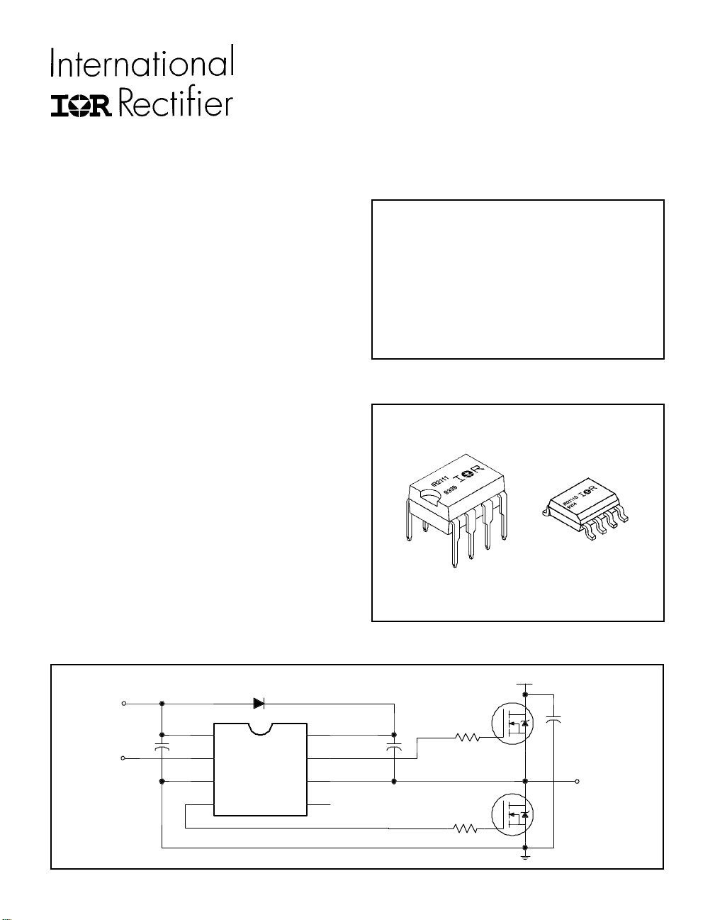
Typical Connection
V
CC
IN
V
CC
IN
COM
LO
up to 600V
V
B
HO
V
S
TO
LOAD
CONTROL INTEGRATED CIRCUIT DESIGNERS MANUAL B-39
IR2111
Next Data SheetIndex
Previous Datasheet
To Order
Absolute Maximum Ratings
Absolute Maximum Ratings indicate sustained limits be yond which damage to the device ma y occur. All voltage parameters are
absolute voltages ref erenced to COM. The Thermal Resistance and P o wer Dissipation r atings are measured under board
mounted and still air conditions. Additional information is shown in Figures 7 through 10.
Par ameter Value
Symbol Definition Min. Max. Units
V
B
V
S
V
HO
V
CC
V
LO
V
IN
dVs/dt Allowable Offset Supply V oltage T ransient (Figure 2) — 50 V/ns
P
D
R
θJA
T
J
T
S
T
L
High Side Floating Supply V oltage -0.3 625
High Side Floating Supply Offset V oltage VB - 25 VB + 0.3
High Side Floating Output V oltage VS - 0.3 V
Low Side and Logic Fix ed Supply V oltage -0.3 25
Low Side Output Voltage -0.3 VCC + 0.3
Logic Input V oltage -0.3 V
P ackage P ow er Dissipation @ TA ≤ +25° C (8 Lead DIP) — 1.0
(8 Lead SOIC) — 0.625
Thermal Resistance, Junction to Ambient (8 Lead DIP) — 12 5
(8 Lead SOIC) — 20 0
Junction Temperature — 150
Storage T emperature -55 150 °C
Lead Temperature (Soldering, 10 seconds) — 3 00
CC
B
+ 0.3
+ 0.3
V
W
°C/W
Recommended Operating Conditions
The Input/Output logic timing diagram is shown in Figure 1. For proper operation the device should be used within the
recommended conditions. The V
Symbol Definition Min. Max. Units
V
B
V
S
V
HO
V
CC
V
LO
V
IN
T
A
Note 1: Logic operational for VS of -5 to +600V. Logic state held for VS of -5V to -VBS.
High Side Floating Supply Absolute V oltage VS + 10 VS + 20
High Side Floating Supply Offset V oltage Note 1 60 0
High Side Floating Output V oltage V
Low Side and Logic Fix ed Supply V oltage 10 20
Low Side Output Voltage 0 V
Logic Input V oltage 0 V
Ambient T emper ature -40 125
B-40 CONTROL INTEGRATED CIRCUIT DESIGNERS MANUAL
offset rating is tested with all supplies biased at 15V differential.
S
Parameter V alue
S
V
B
CC
CC
V
°C
Dynamic Electrical Characteristics
To Order
Next Data SheetIndex
Previous Datasheet
V
(VCC, VBS) = 15V, CL = 1000 pF and TA = 25°C unless otherwise specified. The dynamic electrical characteristics
BIAS
are measured using the test circuit shown in Figure 3.
Parameter Value
Symbol Definition Min. Typ. Max. Units Test Conditions
t
on
t
off
t
t
DT Deadtime, LS Turn-Off to HS Turn-On & — 7 00 900
MT Delay Matching, HS & LS Turn-On/Off — 30 —
Turn-On Propagation Delay — 850 1,000 VS = 0V
Turn-Off Propagation Delay — 150 180 VS = 600V
Turn-On Rise Time — 80 130
r
Turn-Off Fall Time — 40 65
f
HS Turn-Off to LS Turn-On
Static Electrical Characteristics
V
(VCC, VBS) = 15V and TA = 25°C unless otherwise specified. The VIN, VTH and IIN parameters are referenced to
BIAS
COM. The V
Symbol Definition Min. Typ. Max. Units Test Conditions
V
V
V
V
I
I
QBS
I
QCC
I
IN+
I
IN-
V
BSUV+VBS
V
BSUV-
V
CCUV+VCC
V
CCUV-
I
O+
I
and IO parameters are referenced to COM and are applicable to the respective output leads: HO or LO.
O
Parameter Value
Logic “1” Input Voltage for HO & Logic “0” for LO 6.4 — — VCC = 10V
IH
Logic “0” Input Voltage for HO & Logic “1” for LO — — 3.8 VCC = 10V
IL
OH
OL
LK
O-
High Level Output V oltage, V
Low Level Output Voltage , V
Offset Supply Leakage Current — — 50 VB = VS = 600V
Quiescent VBS Supply Current — 50 100 V
Quiescent VCC Supply Current — 70 180 µA VIN = 0V or V
Logic “1” Input Bias Current — 20 40 VIN = V
Logic “0” Input Bias Current — — 1.0 VIN = 0V
Supply Undervoltage Positive Going Threshold 7.3 8.4 9.5
VBS Supply Undervoltage Negative Going Threshold 7.0 8.1 9.2
Supply Undervoltage Positive Going Threshold 7.6 8.6 9.6
VCC Supply Undervoltage Negative Going Threshold 7.2 8.2 9.2
Output High Short Circuit Pulsed Current 200 250 — VO = 0V, V
Output Low Short Circuit Pulsed Current 420 500 — VO = 15V, V
BIAS
O
- V
IR2111
ns
9.5 — — VCC = 15V
12.6 — — VCC = 20V
——6.0 VCC = 15V
——8.3 VCC = 20V
O
— — 100 IO = 0A
— — 100 IO = 0A
V
mV
V
mA
= 0V or V
IN
IN
PW ≤ 10 µs
PW ≤ 10 µs
CC
IN
= V
CC
CC
CC
= 0V
CONTROL INTEGRATED CIRCUIT DESIGNERS MANUAL B-41

IR2111
To Order
Next Data SheetIndex
Previous Datasheet
Functional Block Diagram
DEAD
TIME
HV
LEVEL
SHIFT
UV
DETECT
PULSE
FILTER
V
B
Q
R
R
S
HO
PULSE
GEN
IN
UV
DETECT
DEAD
TIME
Lead Definitions
Lead
Symbol Description
IN Logic input for high side and low side gate driver outputs (HO & LO), in phase with HO
V
B
HO High side gate drive output
V
S
V
CC
LO Low side gate drive output
COM Low side return
High side floating supply
High side floating supply return
Low side and logic fixed supply
V
S
V
CC
LO
COM
Lead Assignments
8 Lead DIP SO-8
IR2111 IR2111S
B-42 CONTROL INTEGRATED CIRCUIT DESIGNERS MANUAL
Part Number

Device Information
To Order
Next Data SheetIndex
Previous Datasheet
Process & Design Rule HVDCMOS 4.0 µm
Transistor Count 164
Die Size 70 X 96 X 26 (mil)
Die Outline
Thickness of Gate Oxide 80 0Å
Connections Material Poly Silicon
First Width 4 µm
Layer Spacing 6 µm
Thickness 5000Å
Material Al - Si (Si: 1.0% ±0.1%)
Second Width 6 µm
Layer Spacing 9 µm
Thickness 20,000Å
Contact Hole Dimension 8 µm X 8 µm
Insulation Layer Material PSG (SiO2)
Thickness 1.5 µm
Passivation Material PSG (SiO2)
Thickness 1.5 µm
Method of Saw Full Cut
Method of Die Bond Ablebond 84 - 1
Wire Bond Method Thermo Sonic
Material Au (1.0 mil / 1.3 mil)
Leadframe Material Cu
Die Area Ag
Lead Plating Pb : Sn (37 : 63)
Pa ckage Types 8 Lead PDIP / SO-8
Materials EME6300 / MP150 / MP190
Remarks:
IR2111
CONTROL INTEGRATED CIRCUIT DESIGNERS MANUAL B-43

IR2111
To Order
Next Data SheetIndex
Previous Datasheet
IN
HO
LO
Figure 1. Input/Output Timing Diagram Figure 2. Floating Supply Voltage Transient Test Circuit
IN
IN
(LO)
(HO)
t
50% 50%
t
on
r
t
off
90% 90%
t
f
Figure 3. Switching Time Test Circuit Figure 4. Switching Time Waveform Definition
50% 50%
IN
90%
HO
LO
Figure 5. Deadtime Waveform Definitions
10%
DT
90%
10%
B-44 CONTROL INTEGRATED CIRCUIT DESIGNERS MANUAL
LO
HO
IN
(LO)
IN
(HO)
Figure 6. Delay Matching Waveform Definitions
10% 10%
50% 50%
LO
MT
HO
10%
MT
90%
HOLO

IR2111
J
)
J
)
)
)
To Order
Next Data SheetIndex
Previous Datasheet
150
125
100
75
50
unction Temperature (°C
25
0
1E+2 1E+3 1E+4 1E+5 1E+6
Figure 7. IR2111 T
R
150
125
100
75
50
Junction Temperature (°C
25
Frequency (Hz)
vs. Frequency (IRFBC20)
J
ΩΩ
= 33
Ω, VCC = 15V
GATE
ΩΩ
320V 140V 10 V
320V
140V
10V
150
125
100
75
50
unction Temperature (°C
25
0
1E+2 1E+3 1E+4 1E+5 1E+6
Figure 8. IR2111 T
R
150
125
100
75
50
Junction Temperature (°C
25
Frequency (Hz)
vs. Frequency (IRFBC30)
J
ΩΩ
= 22
Ω, VCC = 15V
GATE
ΩΩ
320V
140V
320V 140V
10V
10V
0
1E+2 1E+3 1E+4 1E+5 1E+6
Figure 9. IR2111 TJ vs. Frequency (IRFBC40)
R
GATE
Frequency (Hz)
ΩΩ
= 15
Ω, VCC = 15V
ΩΩ
0
1E+2 1E+3 1E+4 1E+5 1E+6
Frequency (Hz)
Figure 10. IR2111 TJ vs. Frequency (IRFPE50)
R
GATE
ΩΩ
= 10
Ω, VCC = 15V
ΩΩ
CONTROL INTEGRATED CIRCUIT DESIGNERS MANUAL B-45
 Loading...