

查询IR2110E6供应商
Data Sheet No. PD-6.065
IR2110E6
HIGH AND LOW SIDE DRIVER
Features
n Floating channel designed for bootstrap operation
Fully operational to +600V
Tolerant to negative transient voltage
dV/dt immune
n Gate drive supply range from 10 to 20V
n Undervoltage lockout for both channels
n Separate logic supply range from 5 to 20V
Logic and power ground ±5V offset
n CMOS Schmitt-triggered inputs with pull-down
n Cycle by cycle edge-triggered shutdown logic
n Matched propagation delay for both channels
n Outputs in phase with inputs
Absolute Maximum Ratings
Absolute Maximum Ratings indicate sustained limits beyond which damage to the device may occur. All voltage parameters are absolute
voltages referenced to COM. The Thermal Resistance and Power Dissipation ratings are measured under board mounted and still air
conditions. Additional information is shown in Figures 28 through 35.
Symbol Parameter Min. Max. Units
V
B
V
S
V
HO
V
CC
V
LO
V
DD
V
SS
V
IN
dVS/dt Allowable Offset Supply Voltage Transient (Fig. 16) — 50 V/ns
P
D
R
thJA
T
j
T
S
T
L
High Side Floating Supply Absolute Voltage -0.5 VS + 20
High Side Floating Supply Offset Voltage — 600
High Side Output Voltage VS -0.5 V
Low Side Fixed Supply Voltage -0.5 20
Low Side Output Voltage -0.5 VCC + 0.5
Logic Supply Voltage -0.5 VSS + 20
Logic Supply Offset Voltage VCC - 20 V
Logic Input Voltage (HIN, LIN & SD) VSS - 0.5 V
Package Power Dissipation @ TA ≤ = 25°C (Fig. 19) — 1.6 W
Thermal Resistance, Junction to Ambient — 75 °C/W
Junction Temperature -55 125
Storage Temperature -55 150
Package Mounting Surface Temperature 300 (for 5 seconds)
Weight
Product Summary
V
OFFSET
+/- 2A / 2A
I
O
V
OUT
t
(typ.) 120 & 94 ns
on/off
Delay Matching 10 ns
600V max.
10 - 20V
Description
The IR2110E6 is a high voltage, high speed
power MOSFET and IGBT driver with independent
high and low side referenced output channels. Proprietary HVIC and latch immune CMOS technologies enable ruggedized monolithic construction.
Logic inputs are compatible with standard CMOS or
LSTTL outputs. The output drivers feature a high
pulse current buffer stage designed for minimum
driver cross-conduction. Propagation delays are
matched to simplify use in high frequency applications. The floating channel can be used to drive an
N-channel power MOSFET or IGBT in the high side
configuration which operates up to 600 volts.
+ 0.5
B
+ 0.5
CC
+ 0.5
DD
0.45 (typical) g
V
°C
IR2110E6
Recommended Operating Conditions
The Input/Output logic timing diagram is shown in Figure 1. For proper operation the device should be used within the
recommended conditions. The VS and VSS offset ratings are tested with all supplies biased at 15V differential. T ypical
ratings at other bias conditions are shown in Figures 36 and 37.
Symbol Parameter Min. Max. Units
V
B
V
S
V
HO
V
CC
V
LO
V
DD
V
SS
V
IN
Dynamic Electrical Characteristics
V
(VCC, VBS, VDD) = 15V, and VSS = COM unless otherwise specified. The dynamic electrical
BIAS
characteristics are measured using the test circuit shown in Figure 3.
Symbol Parameter Min Typ. Max. Min. Max Units Test Conditions
t
on
t
off
t
sd
trTurn-On Rise Time — 25 35 — 50 CL = 1000pf
tfTurn-Off Fall Time — 17 25 — 40 CL = 1000pf
Mt Delay Matching, HS & LS Turn-On/Off — — 10 — —
High Side Floating Supply Absolute Voltage VS + 10 VS + 20
High Side Floating Supply Offset Voltage -4 600
High Side Output Voltage V
S
V
B
Low Side Fixed Supply Voltage 10 20
Low Side Output Voltage 0 V
CC
Logic Supply Voltage VSS + 5 VSS + 20
Logic Supply Offset Voltage -5 5
Logic Input Voltage (HIN, LIN & SD) V
Tj = 25°C
Tj = -55 to
SS
V
DD
125°C
Turn-On Propagation Delay — 120 150 — 260 VS = 0V
Turn-Off Propagation Delay — 94 125 — 220 VS = 600V
Shutdown Propagation Delay — 110 140 — 2 3 5 VS = 600V
ns
Hton-Lt
on
/ Ht
off
-Lt
off
V
Typical Connection
V
DD
HIN
SD
LIN
V
SS
V
CC
V
DD
HIN
SD
LIN
V
SS
HO
V
COM
LO
up to 500V
up to 600V
V
B
V
S
CC
TO
LOAD
IR2110E6
Static Electrical Characteristics
V
(VCC, VBS, VDD) = 15V, unless otherwise specified. The VIN, VTH and IIN parameters are referenced to VSS and
BIAS
are applicable to all three logic input leads: HIN, LIN and SD. The VO and IO parameters are referenced to COM and are
applicable to the respective output leads: HO or LO.
Tj = 25°C
Symbol Parameter Min Typ. Max. Min. Max Units Test Conditions
V
IH
Logic “1” Input Voltage 3.1 — — 3.3 — VDD = 5V
6.4 — — 6.8 — V
9.5 — — 10 — VDD = 15V
12.6 — — 13.3 — V VDD = 20V
V
Logic “0” Input Voltage — — 1.8 — 1.7 VDD = 5V
IL
— — 3.8 — 3.6 VDD = 10V
— — 6 — 5.7 W VDD = 15V
— — 8.3 — 7.9 V VDD = 20
V
V
I
I
I
I
I
I
V
High Level Output Voltage, V
OH
Low Level Output Voltage, VO — — 0.1 — 0.1 VIN = VIL, IO = 0A
OL
Offset Supply Leakage Current — — 50 — 25 0 VB = VS = 600V
LK
Quiescent VBS Supply Current — 125 230 — 5 00 V
QBS
Quiescent VCC Supply Current — 180 340 — 600 V
QCC
Quiescent VDD Supply Current — 5 30 — 60 V
QDD
Logic “1” Input Bias Current — 1 5 40 — 7 0 VIN = V
IN+
Logic “0” Input Bias Current — — 1 — 1 0 VIN = 0V
IN-
BSUV+VBS
Supply Undervoltage Positive 7.5 8.6 9.7 — —
- VO— 0.7 1.2 — 1.5 VIN = VIH, IO = 0A
BIAS
Going Threshold
V
BSUV-VBS
Supply Undervoltage Negative 7.0 8.2 9.4 — —
Going Threshold
V
CCUV+VCC
Supply Undervoltage Positive 7.4 8.5 9.6 — —
Going Threshold
V
CCUV-VCC
Supply Undervoltage Negative 7.0 8.2 9.4 — —
Going Threshold
I
Output High Short Circuit Pulsed 2 ———— V
O+
Current PW < = 10
I
Output Low Short Circuit Pulsed 2 ———— V
O-
Current PW < = 10
Tj = -55 to
125°C
V
V
µA
V
A
= 10V
DD
= 0V or V
IN
= 0V or V
IN
= 0V or V
IN
= 0V, VIN = V
OUT
= 15V, VIN = 0V
OUT
DD
DD
DD
DD
DD
µs
µs
IR2110E6
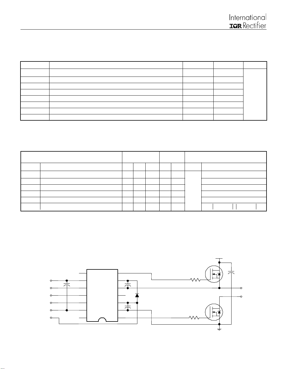
Figure 1. Input/Output Timing Diagram Figure 2. Floating Supply Voltage T ransient Test Circuit
10 to 600V
50%
t
off
90% 90%
t
f
(0 to 600V)
HIN
LIN
50%
t
on
t
r
HO
LO
Figure 3. Switching Time Test Circuit Figure 4. Switching Time Waveform Definition
HIN
LIN
SD
50%
t
sd
HO
90%
LO
10% 10%
50% 50%
LO
MT
HO
10%
MT
90%
HOLO
Figure 5. Shutdown Waveform Definitions
Figure 6. Delay Matching Waveform Definitions
IR2110E6
e (
T
e (
e (
T
e (
S
me
S
e
250
200
150
Max.
Typ.
100
urn-On Delay Tim
50
0
-50 -25 0 25 50 75 100 125
Temperature (°C)
250
200
Max.
Typ.
150
100
Turn-On Delay Tim
50
0
10 12 14 16 18 20
V
Suppl y Voltage (V)
BIAS
Figure 7A. T urn-On Time vs. Temperature Figure 7B. Turn-On Time vs. Voltage
250
200
150
Max.
100
Typ.
Turn-Off Delay Tim
50
250
200
Max.
150
Typ.
100
urn-Off Delay Tim
50
0
-50 -25 0 25 50 75 100 125
Temperature (°C)
0
10 12 14 16 18 20
V
Suppl y Voltage (V)
BIAS
Figure 8A. Turn-Off T ime vs. Temperature Figure 8B. Turn-Off Time vs. Voltage
250
200
150
Max.
100
Typ.
hutdown Delay Tim
50
0
-50 -25 0 25 50 75 100 125
Temperature (°C)
Figure 9A. Shutdown Time vs. Temperature
250
200
Max.
150
Typ.
100
hutdown Delay ti
50
0
10 12 14 16 18 20
V
Suppl y Voltage (V)
BIAS
Figure 9B. Shutdown Time vs. Voltage

IR2110E6
(n
x.
(n
T
(n
T
(n
L
old
L
old
100
80
60
40
Ma
Turn-On Rise Time
Typ.
20
0
-50 -25 0 25 50 75 100 125
Temperature (°C)
Figure 10A. Turn-On Rise Time vs. Temperature
50
40
30
Max.
20
urn-Off Fall Time
Typ.
10
100
80
60
Max.
40
Typ.
Turn-On Rise Time
20
0
10 12 14 16 18 20
V
Suppl y Voltage (V)
BIAS
Figure 10B. Turn-On Rise Time vs. Voltage
50
40
30
20
Max.
urn-Off Fall Time
Typ.
10
0
-50 -25 0 25 50 75 100 125
Temperature (°C)
0
10 12 14 16 18 20
V
Suppl y Voltage (V)
BIAS
Figure 11A. Turn-Off Fall Time vs. T emperature Figure 1 1B. Turn-Off Fall Time vs. Voltage
15.0
12.0
Min.
9.0
6.0
ogic "1" Input Thresh
3.0
0.0
-50 -25 0 25 50 75 100 125
Figure 12A. Logic “1” Input Threshold vs. Temperature Figure 12B. Logic “1” Input Threshold vs. Voltage
Temperature (°C)
15.0
12.0
9.0
6.0
Min.
ogic "1" Input Thresh
3.0
0.0
5 7.5 10 12.5 15 17.5 20
V
Logic Suppl y Vol tage (V)
DD

IR2110E6
L
old
L
old
H
ltag
L
ltag
ltag
x.
L
old
15.0
12.0
9.0
Max.
6.0
ogic "0" Input Thresh
3.0
0.0
-50 -25 0 25 50 75 100 125
Temperature (°C)
15.0
12.0
9.0
6.0
ogic "0" Input Thresh
3.0
Max.
0.0
5 7.5 10 12.5 15 17.5 20
V
Logic Suppl y Vol tage (V)
DD
Figure 13A. Logic “0” Input Threshold vs. Temperature Figure 13B. Logic “0” Input Threshold vs. Voltage
5.00
4.00
3.00
2.00
igh Level Output Vo
Max.
1.00
5.00
4.00
3.00
2.00
Ma
High Level Output Vo
1.00
0.00
-50 -25 0 25 50 75 100 125
Temperature (°C)
0.00
10 12 14 16 18 20
V
Suppl y Voltage (V)
BIAS
Figure 14A. High Level Output vs. Temperature Figure 14B. High Level Output vs. Voltage
1.00
0.80
0.60
0.40
ow Level Output Vo
0.20
Max.
0.00
-50 -25 0 25 50 75 100 125
Temperature (°C)
15.0
12.0
9.0
6.0
Min.
ogic "1" Input Thresh
3.0
0.0
5 7.5 10 12.5 15 17.5 20
V
Logic Suppl y Vol tage (V)
DD
Figure 15B. Low Level Output vs. VoltageFigure 15A. Low Level Output vs. Temperature

IR2110E6
V
t (µ
V
t (µ
V
t (µ
V
t (µ
O
rren
O
rren
500
400
300
200
ffset Supply Leakage Cu
100
Max.
0
-50 -25 0 25 50 75 100 125
500
400
300
Max.
200
BS Supply Curren
Typ.
100
Temperature (°C)
500
400
300
200
ffset Supply Leakage Cu
100
Max.
0
0 100 200 300 400 500
V
Boost Voltage (V)
B
Figure 16B. Offset Supply Current vs. VoltageFigure 16A. Offset Supply Current vs. Temperature
500
400
300
200
BS Supply Curren
Max.
100
Typ.
0
-50 -25 0 25 50 75 100 125
Figure 17A. V
625
500
375
Max.
250
CC Supply Curren
Typ.
125
0
-50 -25 0 25 50 75 100 125
Figure 18A. V
Temperature (°C)
Supply Current vs. Temperature Figure 17B. VBS Supply Current vs. Voltage
BS
Temperature (°C)
Supply Current vs. Temperature Figure 18B. V
CC
0
10 12 14 16 18 20
625
500
375
250
CC Supply Curren
Max.
125
Typ.
0
10 12 14 16 18 20
V
Floating Suppl y Voltage (V)
BS
V
Fixed Supply Voltage (V)
CC
Supply Current vs. Voltage
CC

IR2110E6
V
t (µ
V
t (µ
nt
L
nt
x.Typ.
L
nt
L
nt
100
80
60
40
DD Supply Curren
Max.
20
Typ.
0
-50 -25 0 25 50 75 100 125
Temperature (°C)
Figure 19A. VDD Supply Current vs. Temperature Figure 19B. V
100
80
60
40
Max.
Logic "1" Input Bias Curre
20
Typ.
0
-50 -25 0 25 50 75 100 125
Temperature (°C)
100
80
60
40
DD Supply Curren
Max.
20
Typ.
0
5 7.5 10 12.5 15 17.5 20
V
Logic Suppl y Vol tage (V)
DD
Supply Current vs. Voltage
DD
100
80
60
40
ogic "1" Input Bias Curre
Ma
20
0
5 7.5 10 12.5 15 17.5 20
V
Logic Suppl y Vol tage (V)
DD
Figure 20A. Logic “1” Input Current vs. Temperature Figure 20B. Logic “1” Input Current vs. Voltage
5.00
4.00
3.00
2.00
ogic "0" Input Bias Curre
Max.
1.00
0.00
-50 -25 0 25 50 75 100 125
Temperature (°C)
Figure 21A. Logic “0” Input Current vs. Temperature Figure 21B. Logic “0” Input Current vs. Voltage
5.00
4.00
3.00
2.00
ogic "0" Input Bias Curre
Max.
1.00
0.00
5 7.5 10 12.5 15 17.5 20
V
Logic Suppl y Vol tage (V)
DD

IR2110E6
V
out
out
out
V
out
O
rren
rren
11.0
10.0
Max.
9.0
Typ.
8.0
Min.
VBS Undervoltage Lock
7.0
6.0
-50 -25 0 25 50 75 100 125
Temperature (°C)
11.0
10.0
Max.
9.0
Typ.
8.0
VBS Undervoltage Lock
7.0
Min.
6.0
-50 -25 0 25 50 75 100 125
Temperature (°C)
Figure 22. VBS Undervoltage (+) vs. Temperature Figure 23. VBS Undervoltage (-) vs. Temperature
11.0
10.0
Max.
9.0
Typ.
8.0
Min.
CC Undervoltage Lock
7.0
11.0
10.0
Max.
9.0
Typ.
8.0
CC Undervoltage Lock
7.0
Min.
6.0
-50 -25 0 25 50 75 100 125
Temperature (°C)
Figure 24. V
Undervoltage (+) vs. Temperature Figure 25. VCC Undervoltage (-) vs. Temperature
CC
5.00
4.00
Typ.
3.00
Min.
2.00
Output Source Cu
1.00
0.00
-50 -25 0 25 50 75 100 125
Temperature (°C)
6.0
-50 -25 0 25 50 75 100 125
Temperature (°C)
5.00
4.00
3.00
2.00
Typ.
utput Source Cu
1.00
Min.
0.00
10 12 14 16 18 20
V
Suppl y Voltage (V)
BIAS
Figure 26A. Output Source Current vs. Temperature Figure 26B. Output Source Current vs. Voltage

IR2110E6
O
ent
J
ure
1
V
J
ure
J
ure
J
ure
O
ent
5.00
4.00
Typ.
3.00
Min.
2.00
utput Sink Curr
1.00
0.00
-50 -25 0 25 50 75 100 125
150
125
100
75
50
unction Temperat
25
Temperature (°C)
32 0V
14 0V
10 V
5.00
4.00
3.00
2.00
utput Sink Curr
Typ.
1.00
Min.
0.00
10 12 14 16 18 20
V
Suppl y Voltage (V)
BIAS
Figure 27B. Output Sink Current vs. VoltageFigure 27A. Output Sink Current vs. Temperature
150
125
100
75
50
unction Temperat
25
32 0V
4 0
10 V
0
1E+2 1E+3 1E +4 1E+5 1E+6
Frequency (Hz)
Figure 28. IR2110 TJ vs. Frequency (IRFBC20)
R
GATE
150
125
100
75
50
unction Temperat
25
0
1E+2 1E+3 1E+4 1E +5 1E+6
Figure 30. IR2110 T
R
GATE
ΩΩ
= 33
Ω, VCC = 15V
ΩΩ
Frequency (Hz)
vs. Frequency (IRFBC40)
J
ΩΩ
= 15
Ω, VCC = 15V
ΩΩ
32 0V 14 0V
10 V
0
1E+2 1E+3 1E+4 1E +5 1E+6
Frequency (Hz)
Figure 29. IR2110 TJ vs. Frequency (IRFBC30)
R
GATE
150
125
100
75
50
unction Temperat
25
0
1E+2 1E+3 1E+4 1E +5 1E+6
Figure 31. IR2110 T
R
GATE
ΩΩ
= 22
Ω, VCC = 15V
ΩΩ
Frequency (Hz)
vs. Frequency (IRFPE50)
J
ΩΩ
= 10
Ω, VCC = 15V
ΩΩ
32 0V 14 0V
10 V

IR2110E6
J
ure
J
ure
J
ure
J
ure
V
age
V
ltag
150
125
100
75
50
unction Temperat
25
0
1E+2 1E+3 1E+4 1E +5 1E+6
Frequency (Hz)
32 0V 14 0V
Figure 32. IR2110S TJ vs. Frequency (IRFBC20)
ΩΩ
= 33
Ω, VCC = 15V
ΩΩ
32 0V 140V
150
125
100
75
50
unction Temperat
25
R
GATE
150
125
100
10 V
10 V
75
50
unction Temperat
25
0
1E+2 1E+3 1E+4 1E +5 1E+6
Figure 33. IR2110S T
R
150
125
100
75
50
unction Temperat
25
Frequency (Hz)
vs. Frequency (IRFBC30)
J
ΩΩ
= 22
Ω, VCC = 15V
GATE
ΩΩ
32 0V 14 0V
10 V
32 0V 14 0V 10 V
0
1E+2 1E+3 1E+4 1E +5 1E+6
Frequency (Hz)
Figure 34. IR2110S TJ vs. Frequency (IRFBC40)
R
GATE
0.0
-2.0
Typ.
-4.0
-6.0
S Offset Supply Volt
-8.0
-10.0
10 12 14 16 18 20
Figure 36. Maximum V
V
ΩΩ
= 15
Ω, VCC = 15V
ΩΩ
V
Floating Supply Voltage (V)
BS
Negative Offset vs.
S
Supply Voltage
BS
0
1E+2 1E+3 1E+4 1E +5 1E+6
Frequency (Hz)
Figure 35. IR2110S TJ vs. Frequency (IRFPE50)
R
GATE
20.0
16.0
12.0
8.0
Typ.
SS Logic Supply Offset Vo
4.0
0.0
10 12 14 16 18 20
Figure 37. Maximum V
V
ΩΩ
= 10
Ω, VCC = 15V
ΩΩ
V
Fixed Supply Vo ltag e (V)
CC
Positive Offset vs.
SS
Supply Voltage
CC

Functional Block Diagram
V
DD
HIN
SD
LIN
V
RSQ
RSQ
SS
VDD/V
LEVEL
SHIFT
VDD/V
LEVEL
SHIFT
IR2110E6
V
UV
DETECT
HV
LEVEL
CC
PULSE
GEN
CC
SHIFT
PULSE
FILTER
RQ
R
S
UV
DETECT
DELAY
B
HO
V
S
V
CC
LO
COM
Lead Definitions
Lead
Symbol Description
V
DD
HIN Logic input for high side gate driver output (HO), in phase
SD Logic input for shutdown
LIN Logic input for low side gate driver output (LO), in phase
V
SS
V
B
HO High side gate drive output
V
S
V
CC
LO Low side gate drive output
COM Low side return
Logic supply
Logic ground
High side floating supply
High side floating supply return
Low side supply

IR2110E6
Case Outline and Dimensions — LCC
PAD ASSIGNMENTS
1—Lo
2 — COMM
4—V
6—V
8—VB
9—Ho
11 — V
13 — HIN
14 — SD
15 — LIN
17 — V
3, 5
7, 10
12,16
& 18
CC
S
DD
SS
NO CONNECTION
}
WORLD HEADQUARTERS: 233 Kansas St., El Segundo, California 90245, Tel: (310) 322 3331
EUROPEAN HEADQUARTERS: Hurst Green, Oxted, Surrey RH8 9BB, UK Tel: (44) 0883 713215
IR CANADA: 7321 Victoria Park Ave., Suite 201, Markham, Ontario L3R 3L1, Tel: (905) 475 1897
IR FAR EAST: K&H Bldg., 2F, 3-30-4 Nishi-Ikeburo 3-Chome, Toshima-Ki, Tokyo 171 Tel: (03)3983 0641
IR SOUTHEAST ASIA: 315 Outram Road, #10-02 Tan Boon Liat Building, Singapore 0316 Tel: 65 221 8371
IR GERMANY: Saalburgstrasse 157, 61350 Bad Homburg Tel: 6172 37066
IR ITALY: Via Liguria 49, 10071 Borgaro, Torino Tel: (39) 1145 10111
http://www/irf.com/
Data and specifications subject to change without notice. 9/96
 Loading...