

查询IR2106供应商
Data Sheet No. PD60162 Rev. V
IR2106(4)
(S)
HIGH AND LOW SIDE DRIVER
Features
Floating channel designed for bootstrap operation
•
Fully operational to +600V
Tolerant to negative transient voltage
dV/dt immune
Gate drive supply range from 10 to 20V (IR2106(4))
•
Undervoltage lockout for both channels
•
3.3V, 5V and 15V input logic compatible
•
Matched propagation delay for both channels
•
Logic and power ground +/- 5V offset.
•
Lower di/dt gate driver for better noise immunity
•
Outputs in phase with inputs (IR2106)
•
Description
The IR2106(4)(S) are high voltage,
high speed power MOSFET and
IGBT drivers with independent high
and low side referenced output channels. Proprietary HVIC and latch
immune CMOS technologies enable
ruggedized monolithic construction.
The logic input is compatible with
standard CMOS or LSTTL output,
down to 3.3V logic. The output driv-
2106/2301//2108//2109/2302/2304
Part
2106/2301
21064
2108 Internal 540ns COM
21084
2109/2302 Internal 540ns COM
21094
2304
ers feature a high pulse current buffer stage designed for minimum driver cross-conduction. The floating
channel can be used to drive an N-channel power MOSFET or IGBT in the high side configuration which
operates up to 600 volts.
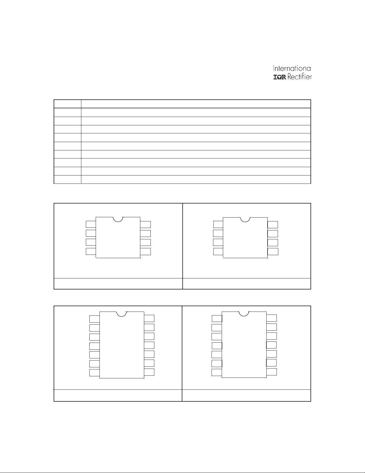
Packages
8-Lead SOIC
14-Lead SOIC
Input
logic
HIN/LIN no none
HIN/LIN yes
IN/SD yes
HIN/LIN
Crossconduction
prevention
logic
yes
Dead-Time Ground Pins Ton/Toff
Programmable 0.54~5 µs
Programmable 0.54~5 µs
Internal 100ns
8-Lead PDIP
14-Lead PDIP
Feature Comparison
COM
VSS/COM
VSS/COM
VSS/COM
COM
220/200
220/200
750/200
160/140
Typical Connection
V
CC
V
V
CC
HIN
LIN
(Refer to Lead Assignments for correct pin configuration). This/These
diagram(s) show electrical connections only. Please refer to our Application Notes and DesignTips for
proper circuit board layout.
HIN
LIN
HO
V
LOCOM
B
S
IR2106
up to 600V
TO
LOAD
up to 600V
HO
V
V
CC
HIN
LIN
V
SS
HIN
LIN
V
V
CC
B
V
S
IR21064
COM
SS
LO
TO
LOAD
www.irf.com 1
IR2106(4)
(S)
Absolute Maximum Ratings
Absolute maximum ratings indicate sustained limits beyond which damage to the device may occur. All voltage parameters are absolute voltages referenced to COM. The thermal resistance and power dissipation ratings are measured
under board mounted and still air conditions.
Symbol Definition Min. Max. Units
V
B
V
S
V
HO
V
CC
V
LO
V
IN
V
SS
dVS/dt Allowable offset supply voltage transient — 50 V/ns
P
D
Rth
JA
T
J
T
S
T
L
High side floating absolute voltage -0.3 625
High side floating supply offset voltage VB - 25 VB + 0.3
High side floating output voltage VS - 0.3 V
Low side and logic fixed supply voltage -0.3 25
Low side output voltage -0.3 VCC + 0.3
Logic input voltage VSS - 0.3 V
Logic ground (IR21064 only) V
Package power dissipation @ TA ≤ +25°C (8 lead PDIP) — 1.0
(8 lead SOIC) — 0.625
(14 lead PDIP) — 1.6
(14 lead SOIC) — 1.0
Thermal resistance, junction to ambient (8 lead PDIP) — 125
(8 lead SOIC) — 200
(14 lead PDIP) — 75
(14 lead SOIC) — 120
Junction temperature — 150
Storage temperature -50 150
Lead temperature (soldering, 10 seconds) — 300
- 25 V
CC
CC
CC
B
+ 0.3
+ 0.3
+ 0.3
°C/W
V
W
°C
2 www.irf.com
IR2106(4)
Recommended Operating Conditions
The Input/Output logic timing diagram is shown in figure 1. For proper operation the device should be used within the
recommended conditions. The V
Symbol Definition Min. Max. Units
VB High side floating supply absolute voltage IR2106(4) VS + 10 VS + 20
V
S
V
HO
V
CC
V
LO
V
IN
V
SS
T
A
Note 1: Logic operational for VS of -5 to +600V. Logic state held for VS of -5V to -VBS. (Please refer to the Design Tip
DT97-3 for more details).
High side floating supply offset voltage Note 1 600
High side floating output voltage V
Low side and logic fixed supply voltage IR2106(4) 10 20
Low side output voltage 0 V
Logic input voltage VSS V
Logic ground (IR21064 only) -5 5
Ambient temperature -40 125 °C
Dynamic Electrical Characteristics
V
(VCC, VBS) = 15V, VSS = COM, CL = 1000 pF, TA = 25°C.
BIAS
and VSS offset rating are tested with all supplies biased at 15V differential.
S
S
V
B
CC
CC
V
(S)
Symbol Definition Min. Typ. Max. Units Test Conditions
t
on
t
off
MT Delay matching, HS & LS turn-on/off — 0 30
t
t
www.irf.com 3
Turn-on propagation delay — 220 300 VS = 0V
Turn-off propagation delay — 200 280 VS = 0V or 600V
nsec
Turn-on rise time — 1 5 0 220 VS = 0V
r
Turn-off fall time — 50 80 VS = 0V
f
IR2106(4)
(S)
Static Electrical Characteristics
V
(VCC, VBS) = 15V, VSS = COM and TA = 25°C unless otherwise specified. The VIL, VIH and IIN parameters are
BIAS
referenced to VSS/COM and are applicable to the respective input leads. The VO, IO and Ron parameters are referenced to
COM and are applicable to the respective output leads: HO and LO.
Symbol Definition Min. Typ. Max. Units Test Conditions
V
V
V
V
I
I
QBS
I
QCC
I
IN+
I
V
CCUV+
V
BSUV+
V
CCUV-
V
BSUV-
V
CCUVH
V
BSUVH
I
I
OH
OL
LK
IN-
O+
O-
Logic “1” input voltage (IR2106(4))
IH
Logic “0” input voltage (IR2106(4)) —
IL
High level output voltage, V
Low level output voltage, V
BIAS
O
- V
O
2.9
— 0.8 1.4 IO = 20 mA
— 0.3 0.6 IO = 20 mA
Offset supply leakage current — — 50 VB = VS = 600V
Quiescent VBS supply current 20 75 1 30 V
Quiescent VCC supply current 60 120 180 VIN = 0V or 5V
Logic “1” input bias current
VIN = 5V (IR2106(4))
—
Logic “0” input bias current
VCC and V
VIN = 0V (IR2106(4))
supply undervoltage positive going 8.0 8.9 9.8
BS
—
threshold
VCC and VBS supply undervoltage negative going 7.4 8.2 9.0
threshold
Hysteresis 0.3 0.7 —
Output high short circuit pulsed current 120 200 — VO = 0V ,
Output low short circuit pulsed current 250 350 — VO = 15V ,
—
—
5
—
—
20
2
0.8
V
µA
V
mA
VCC = 10V to 20V
= 10V to 20V
V
CC
= 0V or 5V
IN
PW ≤ 10 µs
PW ≤ 10 µs
4 www.irf.com
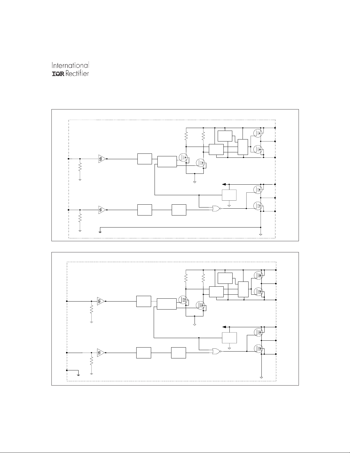
Functional Block Diagrams
IR2106
HIN
LIN
VSS/COM
LEVEL
SHIFT
VSS/COM
LEVEL
SHIFT
PULSE
GENERATOR
DELAY
HV
LEVEL
SHIFTER
PULSE
FILTER
UV
DETECT
DETECT
IR2106(4)
R
RSQ
UV
(S)
VB
HO
VS
VCC
LO
COM
VB
PULSE
FILTER
UV
DETECT
R
Q
R
S
HO
VS
HIN
IR21064
VSS/COM
LEVEL
SHIFT
PULSE
GENERATOR
HV
LEVEL
SHIFTER
VCC
UV
LIN
VSS/COM
LEVEL
SHIFT
DETECT
DELAY
LO
COM
VSS
www.irf.com 5
IR2106(4)
(S)
Lead Definitions
Symbol Description
HIN Logic input for high side gate driver output (HO), in phase
LIN Logic input for low side gate driver output (LO), in phase
VSS Logic Ground (IR21064 only)
V
B
HO High side gate drive output
V
S
V
CC
LO Low side gate drive output
COM Low side return
High side floating supply
High side floating supply return
Low side and logic fixed supply
Lead Assignments
1
V
CC
2
HIN
3
LIN
4
COM
V
HO
V
LO
8
B
7
6
S
5
V
1
HIN
2
LIN
3
COM
4
8 Lead PDIP 8 Lead SOIC
IR2106 IR2106S
V
HO
V
14
13
B
12
11
S
10
9
8
V
1
CC
HIN
2
LIN
3
4
VSS
5
COM
6
LO
7
14 Lead PDIP 14 Lead SOIC
V
1
CC
HIN
2
LIN
3
4
VSS
5
COM
6
LO
7
IR21064 IR21064S
CC
HO
V
HO
V
V
V
LO
8
B
7
6
S
5
14
13
B
12
11
S
10
9
8
6 www.irf.com
HIN
LIN
HO
LO
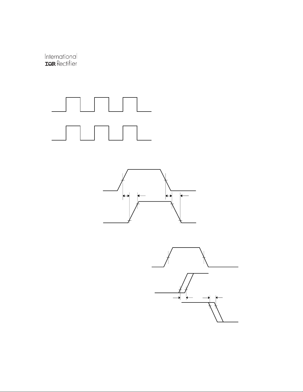
Figure 1. Input/Output Timing Diagram
IR2106(4)
(S)
HIN
50%
50%
LIN
t
on
t
r
90% 90%
t
off
t
f
HO
LO
Figure 2. Switching Time Waveform Definitions
10% 10%
HIN
50%
LIN
MT
LO
50%
HO
10%
MT
90%
HOLO
Figure 3. Delay Matching Waveform Definitions
www.irf.com 7

IR2106(4)
(S)
500
400
300
Max
200
Typ.
100
Turn-on Propagation Delay (ns)
0
-50 -25 0 25 50 75 100 125
Temperature (oC)
Figure 4A. Turn-on Propagation Delay
vs. Temperature
500
400
500
400
M ax.
300
Typ.
200
100
Turn-on Propagation Delay (ns)
0
10 12 14 16 18 20
V
Supply Voltage (V)
BIAS
Figure 4B. Turn-on Propagation Delay
vs. Supply Voltage
500
400
300
M ax.
200
Typ.
100
Turn-of f Propagation Delay (ns)
0
-50 -25 0 25 50 75 100 125
Temper ature (oC)
Figure 5A. Turn-off Propagation Delay
vs. Temperature
M ax.
300
Typ.
200
100
Turn-of f Propagation Delay (ns)
0
10 12 14 16 18 20
V
Supply Voltage (V)
BIAS
Figure 5B. Turn-off Propagation Delay
vs. Supply Voltage
8 www.irf.com

IR2106(4)
(S)
500
400
300
200
M ax.
Typ.
100
Tur n -on Ris e Time (ns)
0
-50 -25 0 25 50 75 100 125
Temperature (oC)
Figure 6A. Turn-on Rise Time
vs. Temperature
200
150
500
400
300
Max.
Typ.
200
100
Turn-on Rise Time (ns )
0
10 12 14 16 18 20
V
Supply Voltage (V)
BIAS
Figure 6B. Turn-on Rise Time
vs. Supply Voltage
200
150
100
Max.
50
Tur n-of f Fall Time ( ns)
Typ.
0
-50-25 0 25 50 75100125
Temperature (oC)
Figure 7A. Turn-off Fall Time
vs. Temperature
Max.
100
Typ.
50
Tur n- of f Fall Time (ns )
0
10 12 14 16 18 20
V
Supply V oltage ( V )
BIAS
Figure 7B. Turn-off Fall Time
vs. Supply Voltage
www.irf.com 9

IR2106(4)
(S)
8
7
6
5
4
Max.
3
Input V oltage (V )
2
1
0
-50 -25 0 25 50 75 100 125
Temper ature (oC)
Figure 8A. Logic “1” Input Voltage
vs. Temperature
4.0
3.2
8
7
6
5
4
Max.
3
Input Voltage (V)
2
1
0
10 12 14 16 18 20
VCC Supply Voltage (V )
Figure 8B. Logic “1” Input Voltage
vs. Supply Voltage
4.0
3.2
2.4
1.6
Input V oltage (V )
Min.
0.8
0.0
-50 -25 0 25 50 75 100 125
Temper ature (oC)
Figure 9A. Logic “0” Input Voltage
vs. Temperature
2.4
1.6
Input Voltage (V)
Min.
0.8
0.0
10 12 14 16 18 20
VCC Supply Voltage (V )
Figure 9B. Logic “0” Input Voltage
vs. Supply Voltage
10 www.irf.com

IR2106(4)
(S)
4
3
2
Max.
1
Typ.
High Level Output Voltage (V)
0
-50 -25 0 25 50 75 100 125
Temperature (oC)
Figure 10A. High Level Output Voltage
vs. Temperature
1.5
1.2
4
3
Max.
2
Typ.
1
High Level Output Voltage (V)
0
10 12 14 16 18 20
V
Supply V oltage ( V )
BIAS
Figure 10B. High Level Output Voltage
vs. Supply Voltage
1.5
1.2
0.9
0.6
Max.
0.3
Typ.
Low Level Output Voltage (V )
0
-50-25 0 255075100125
Temperature (oC)
Figure 11A. Low Level Output Voltage
vs. Temperature
0.9
Max.
0.6
Typ.
0.3
Low Level Output Voltage (V)
0
10 12 14 16 18 20
V
Supply Voltage (V )
BIAS
Figure 11B. Low Level Output Voltage
vs. Supply Voltage
www.irf.com 11

IR2106(4)
.
(S)
500
400
300
200
100
M ax.
Off set Supply Leakage Current ( A)
0
-50 -25 0 25 50 75 100 125
Temper ature (oC)
Figure 12A. Offset Supply Leakage Current
vs. Temperature
400
300
500
400
300
200
100
Max.
Off s et Supply Leakage Current ( A)
0
0 100 200 300 400 500 600
VB Boost V oltage (V)
Figure 12B. Offset Supply Leakage Current
vs. Supply Voltage
400
300
200
M ax.
Supply Current ( A)
100
BS
V
Typ.
Min.
0
-50 -25 0 25 50 75 100 125
Temper ature (oC)
Figure 13A. VBS Supply Current
vs. Temperature
200
Max.
Supply Current ( A)
100
BS
V
Typ.
Min
0
10 12 14 16 18 20
VBS Supply Voltage (V)
Figure 13B. VBS Supply Current
vs. Supply Voltage
12 www.irf.com

IR2106(4)
.
(S)
400
300
200
Max.
Typ.
100
V cc Supply Cur rent ( A)
Min.
0
-50 -25 0 25 50 75 100 125
Tem per atur e (oC)
Figure 14A. Quiescent VCC Supply Current
vs. Temperature
60
50
400
300
200
Supply Current ( A)
100
CC
V
0
10 12 14 16 18 20
VCC Supply Voltage (V)
Figure 14B. Quiescent VCC Supply Current
vs. V
60
50
Supply Voltage
CC
Max
Typ.
Min.
40
30
20
Max.
10
Logic "1" Input Current ( A)
Typ.
0
-50 -25 0 25 50 75 100 125
Temper ature (oC)
Figure 15A. Logic “1” Input Current
vs. Temperature
40
30
Max.
20
10
Logic "1" Input Current ( A)
Typ.
0
10 12 14 16 18 20
VCC Supply Voltage (V )
Figure 15B. Logic “1” Bias Current
vs. Supply Voltage
www.irf.com 13

IR2106(4)
(S)
5
4
3
Max.
2
1
Logic "0" Input Curr ent ( A)
0
-50 -25 0 25 50 75 100 125
Temperature (oC)
Figure 16A. Logic “0” Input Current
vs. Temperature
12
11
5
4
3
M ax.
2
1
Logic "0" Input Current ( A)
0
10 12 14 16 18 20
VCC Supply V oltage (V)
Figure 16B. Logic “0” Input Currentt
vs. Supply Voltage
11
10
10
M ax.
Typ.
9
Min.
UVLO Threshold (+) (V)
8
CC
V
7
-50 -25 0 25 50 75 100 125
Temper ature (oC)
Figure 17. VCC Undervoltage Threshold (+)
vs. Temperature
Max.
9
Typ.
8
Min.
UVLO Threshold (-) (V )
7
CC
V
6
-50 -25 0 25 50 75 100 125
Temper ature (oC)
Figure 18. VCC Undervoltage Threshold (-)
vs. Temperature
14 www.irf.com

IR2106(4)
(S)
12
11
M ax.
10
Typ.
9
Min.
UVLO Threshold (+) (V)
8
BS
V
7
-50 -25 0 25 50 75 100 125
Temper ature (oC)
Figure 19. VBS Undervoltage Threshold (+)
vs. Temperature
500
400
11
10
Max.
9
Typ.
8
Min.
7
UV LO Threshold (-) (V)
BS
V
6
-50 -25 0 25 50 75 100 125
Temper ature (oC)
Figure 20. VBS Undervoltage Threshold (-)
vs. Temperature
500
400
300
Typ.
200
Min.
100
Output Source Current ( A)
0
-50 -25 0 25 50 75 100 125
Temper ature (oC)
Figure 21A. Output Source Current
vs. Temperature
300
200
Typ.
100
Output Source Current ( A)
Min.
0
10 12 14 16 18 20
V
Supply Voltage (V)
BIAS
Figure 21B. Output Source Current
vs. Supply Voltage
www.irf.com 15

IR2106(4)
(S)
600
500
Typ.
400
Min.
300
200
100
Output Sink Current ( A)
0
-50 -25 0 25 50 75 100 125
Temper ature (oC)
Figure 22A. Output Sink Current
vs. Temperature
0
-2
Typ.
-4
-6
-8
Offset Supply Voltage (V)
S
V
-1 0
10 12 14 16 18 20
V
Floating Supply Voltage (V)
BS
600
500
400
300
Typ.
200
Min.
100
Output Sink Current ( A)
0
10 12 14 16 18 20
V
Supply Voltage (V)
BIAS
Figure 22B. Output Sink Currentt
vs. Supply Voltage
140
120
C)
100
o
80
60
Temprature (
40
20
1 10 100 1000
Frequency (KHz)
140V
70V
0V
Figure 23. Maximum VS Negative Offset
vs. Supply Voltage
Figure 24. IR2106 vs. Frequency (IRFBC20),
Rgate=33
ΩΩ
Ω, VCC=15V
ΩΩ
16 www.irf.com

IR2106(4)
(S)
140
120
C)
o
100
80
60
Temperature (
40
20
1 10 100 1000
Frequency (KHz)
Figure 25. IR2106 vs. Freque ncy (IRFBC30),
R
=22Ω, VCC=15V
gate
140
120
C)
o
100
1 40V 70V
140V
70V
0V
140
120
C)
o
100
80
60
Temperature (
40
140V
70V
0V
20
1 10 100 1000
Frequency (KHz)
Figure 26. IR2106 vs. Freque ncy (IRFBC40),
R
=15Ω, VCC=15V
gate
140
0V
120
C)
o
100
80
60
Temperature (
40
20
1 10 100 1000
Frequency ( KHz)
Figure 27. IR2106 vs. Freque ncy (IRFPE50),
=10Ω, VCC=15V
R
gate
80
60
Temperature (
40
20
1 10 100 1000
Frequency (KHz)
Figur e 28. IR21064 vs. Freque ncy (IRFBC20),
=33Ω, VCC=15V
R
gate
140V
70V
0V
www.irf.com 17

IR2106(4)
g
g
(S)
140
120
C)
o
100
80
60
Temperature (
40
20
1 10 100 1000
Frequency (KHz)
Figure 29. IR21064 vs. Freque ncy (IRFBC30),
=22Ω, VCC=15V
R
gate
140
120
C)
o
100
80
60
Temperature (
40
140V
140V
70V
0V
70V
0V
140
120
C)
o
100
80
60
Temperature (
40
20
1 10 100 1000
Frequency (KHz)
Figure 30. IR21064 vs. Freque ncy (IRFBC40),
R
=15Ω, VCC=15V
ate
140
120
C)
o
100
80
60
Temperature (
40
140V
70V
0V
140V
70V
0V
20
1 10 100 1000
Frequency (KHz)
Figure 31. IR21064 vs. Freque ncy ( IRFPE50),
R
=10Ω, V
=15V
20
1 10 100 1000
Frequency (KHz)
Figure 32. IR2106S vs . Frequency (IRFBC20),
R
=33Ω, VCC=15V
ate
18 www.irf.com

IR2106(4)
g
g
(S)
140
120
C)
100
o
80
60
Temperature (
40
20
1 10 100 1000
Frequency (KHz)
Figur e 33. IR2106S vs. Freque ncy (IRFBC30),
=22Ω, VCC=15V
R
gate
140
140V 70V 0V
120
C)
o
100
140V
70V
0V
140
120
C)
o
100
80
60
Temperature (
40
20
1 10 100 1000
Frequency (KHz)
Figur e 34. IR2106S vs. Freque ncy (IRFBC40),
=15Ω, VCC=15V
R
ate
140
120
C)
o
100
140V 70V
0V
80
60
Tempreture (
40
20
1 10 100 1000
Frequency (KHz)
Figure 35. IR2106S vs . Frequency
(IRFPE50), R
=10Ω, VCC=15V
ate
80
60
Temperature (
40
20
1 10 100 1000
Frequency (KHz)
Figure 36. IR21064S vs. Freque ncy (IRFBC20),
=33Ω, VCC=15V
R
gate
140V
70V
0V
www.irf.com 19

IR2106(4)
(S)
140
120
C)
o
100
80
60
Temperature (
40
20
1 10 100 1000
Frequency (KHz)
Figure 37. IR21064S vs. Freque ncy (IRFBC30),
=22Ω, VCC=15V
R
gate
140
120
C)
o
100
140V
70V
0V
140
120
C)
o
100
80
60
Temperature (
40
20
1 10 100 1000
Frequency (KHz)
Figure 38. IR21064S vs . Fre quency (IRFBC40),
=15Ω, VCC=15V
R
gate
140V 70V
0V
1 40V
70V
0V
80
60
Temperature (
40
20
1 10 100 1000
Frequency (KHz)
Figure 39. IR21064S vs . Fre que ncy (IRFPE50),
=10Ω, VCC=15V
R
gate
20 www.irf.com

Case Outlines
IR2106(4)
(S)
A
87
6
E
e
6X
8X b
0.25 [.010] C A B
NOTES:
1. DIMENS ION ING & TOLER ANC ING PER AS ME Y14.5M-1994.
2 . C ON TR O LL IN G D IME N SIO N : M ILL IM ET ER
3. DIME NSIONS ARE SHOWN IN MILLIMETERS [INC HES].
4. OUTLINE C ONFORM S TO J EDEC OU TLINE MS-012AA.
D B
5
65
4312
e1
A1
H
0.25 [.010] A
A
C
0.10 [.004]
8 Lead PDIP
6.46 [.255]
3X 1.27 [.050]
y
8 Lead SOIC
01-3003 01
DIM
FOOTPRINT
8X 0.72 [.028]
8X 1.78 [.070]
MIN MAX
A
.0532
A1
b
c .0075 .0098 0.19 0.25
D
E
e
e1
H
K
L
y
.0688
.0040
.0098
.013
.020
.189
.1968
.1497
.1574
.050 B ASIC
.025 B ASIC 0.635 B ASIC
.2284
.2440
.0099
.0196
.016
.050
0°
K x 45°
8X L
8X c
7
5 DIMENSION DOES NOT INCLUDE MOLD PRO TRUSIONS.
MO LD P ROTRU SIONS NOT TO E XCE ED 0.15 [.0 06].
6 DIMENSION DOES NOT INCLUDE MOLD PRO TRUSIONS.
MO LD P ROTRU SIONS NOT TO E XCE ED 0.25 [.0 10].
7 DIME NS IO N IS THE L ENG TH OF L EA D FOR SO LD ER ING TO
A SU BSTRA TE.
01-0021 11
8°
01-6014
(MS-001AB)
MILLIMETERSIN C H E S
MIN MAX
1.35
1.75
0.10
0.25
0.33
0.51
4.80
5.00
3.80
4.00
1.27 BA SIC
5.80
6.20
0.25
0.50
0.40
1.27
8°
0°
01-6027
(MS-012AA)
www.irf.com 21

IR2106(4)
(S)
14 Lead PDIP
01-3002 03
01-6010
(MS-001AC)
14 Lead SOIC (narrow body)
IR WORLD HEADQUARTERS: 233 Kansas St., El Segundo, California 90245 Tel: (310) 252-7105
Data and specifications subject to change without notice. 1/27/2004
22 www.irf.com
01-3063 00
01-6019
(MS-012AB)
 Loading...