

查询IR2101供应商
Preliminary Data Sheet No. PD60043J
IR2101/IR21014
IR2102/IR21024
HIGH AND LOW SIDE DRIVER
Features
• Floating channel designed for bootstrap operation
Fully operational to +600V
Tolerant to negative transient voltage
dV/dt immune
• Gate drive supply range from 10 to 20V
• Undervoltage lockout
• 5V Schmitt-triggered input logic
• Matched propagation delay for both channels
• Outputs in phase with inputs (IR2101/IR21014) or
out of phase with inputs (IR2102/IR21024)
Description
The IR2101/IR21014/IR2102/IR21024 are high voltage,
high speed power MOSFET and IGBT drivers with independent high and low side referenced output channels. Proprietary HVIC and latch immune CMOS technologies enable ruggedized monolithic construction. The
logic input is compatible with standard CMOS or LSTTL
output. The output drivers feature a high pulse current
buffer stage designed f or minimum driver cross-conduction. The floating channel can be used to drive an Nchannel power MOSFET or IGBT in the high side configuration which operates up to 600 volts.
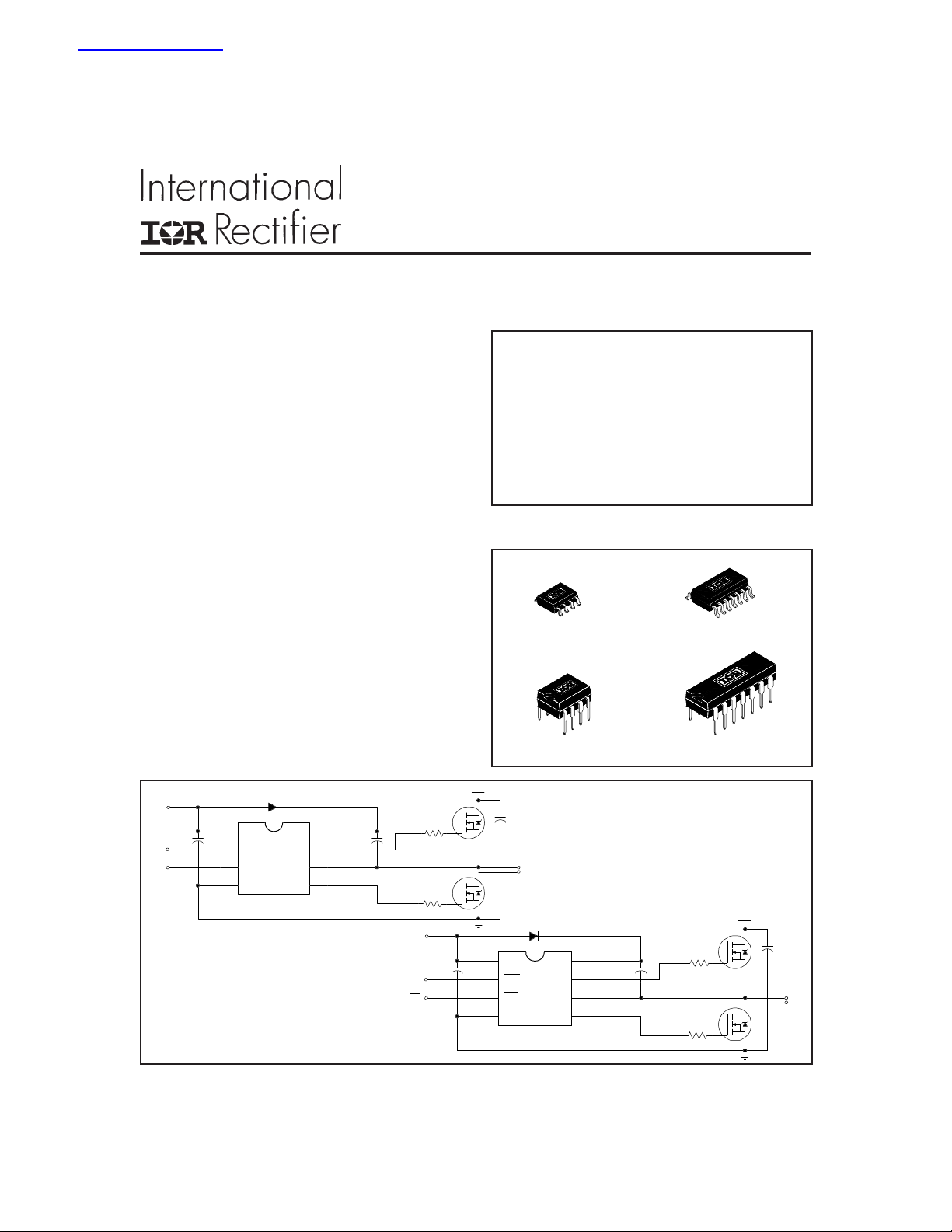
T ypical Connection
V
CC
V
HIN
LIN
HIN
LIN
IR2101
V
CC
HO
LOCOM
B
V
S
V
CC
HIN
LIN
Product Summary
V
OFFSET
IO+/- 130 mA / 270 mA
V
OUT
t
(typ.) 160 & 150 ns
on/off
Delay Matching 50 ns
Packages
8 Lead SOIC 14 Lead SOIC
8 Lead PDIP
up to 600V
TO
LOAD
V
HIN
LIN
CC
IR2102
HO
LOCOM
V
B
V
S
600V max.
10 - 20V
14 Lead PDIP
up to 600V
TO
LOAD
IR2101/IR21014/IR2102/IR21024
Absolute Maximum Ratings
Absolute maximum ratings indicate sustained limits beyond which damage to the device may occur. All voltage parameters are absolute voltages referenced to COM. The thermal resistance and power dissipation ratings are measured
under board mounted and still air conditions.
Symbol Definition Min. Max. Units
V
B
V
S
V
HO
V
CC
V
LO
V
IN
dVS/dt Allowable offset supply voltage transient — 50 V/ns
P
D
Rth
JA
T
J
T
S
T
L
High side floating supply voltage -0.3 625
High side floating supply offset voltage VB - 25 VB + 0.3
High side floating output voltage VS - 0.3 V
Low side and logic fixed supply voltage -0.3 25
Low side output voltage -0.3 VCC + 0.3
Logic input voltage (HIN & LIN) -0.3 V
Package power dissipation @ TA ≤ +25°C (8 lead PDIP) — 1.0
(8 lead SOIC) — 0.625
(14 lead PDIP) — 1.6
(14 lead SOIC) — 1. 0
Thermal resistance, junction to ambient (8 lead PDIP) — 125
(8 lead SOIC ) — 200
(14 lead PDIP) — 75
(14 lead SOIC) — 120
Junction temperature — 150
Storage temperature -55 150
Lead temperature (soldering, 10 seconds) — 300
CC
B
+ 0.3
+ 0.3
W
°C/W
°C
V
Recommended Operating Conditions
The input/output logic timing diagram is shown in figure 1. For proper operation the device should be used within the
recommended conditions. The VS offset rating is tested with all supplies biased at 15V differential.
Symbol Definition Min. Max. Units
V
B
V
S
V
HO
V
CC
V
LO
V
IN
T
A
Note 1: Logic operational for VS of -5 to +600V. Logic state held for VS of -5V to -VBS.
High side floating supply absolute voltage VS + 10 VS + 20
High side floating supply offset voltage Note 1 600
High side floating output voltage V
Low side and logic fixed supply voltage 10 20
Low side output voltage 0 V
Logic input voltage (HIN & LIN) (IR2101) & (HIN & LIN) (IR2102) 0 V
Ambient temperature -40 125
S
V
B
CC
CC
2
°C
V
IR2101/IR21014/IR2102/IR21024
Dynamic Electrical Characteristics
V
(VCC, VBS) = 15V, CL = 1000 pF and TA = 25°C unless otherwise specified.
BIAS
Symbol Definition Min. Typ. Max. Units T est Conditions
t
on
t
off
t
t
MT Delay matching, HS & LS turn-on/off — — 50
Static Electrical Characteristics
V
(VCC, VBS) = 15V and TA = 25°C unless otherwise specified. The VIN, VTH and IIN parameters are referenced to
BIAS
COM. The VO and IO parameters are referenced to COM and are applicable to the respective output leads: HO or LO.
Symbol Definition Min. Typ. Max. Units T est Conditions
V
V
V
OH
V
OL
I
LK
I
QBS
I
QCC
I
IN+
I
IN-
V
CCUV+
V
CCUV-
I
O+
I
O-
Turn-on propagation delay — 160 220 VS = 0V
Turn-off propagation delay — 1 50 220 VS = 600V
Turn-on rise time — 100 170 ns
r
Turn-off fall time — 50 90
f
Logic “1” input voltage (IR2101)
IH
Logic “0” input voltage (IR2102)
Logic “0” input voltage (IR2101)
IL
Logic “1”input voltage (IR2102)
High level output voltage, V
Low level output voltage, V
Offset supply leakage current — — 50 VB = VS = 600V
Quiescent VBS supply current — 30 55 V
Quiescent VCC supply current — 150 270 VIN = 0V or 5V
Logic “1” input bias current
Logic “0” input bias current
VCC supply undervoltage positive going 8 8. 9 9.8
threshold
VCC supply undervoltage negative going 7.4 8.2 9
threshold
Output high short circuit pulsed current 130 210 — VO = 0V
Output low short circuit pulsed current 270 36 0 — VO = 15V
BIAS
O
- V
O
3
—
— — 100 IO = 0A
— — 100 IO = 0A
—
—
—
—
3
—
VCC = 10V to 20V
—
V
VCC = 10V to 20V
0.8
mV
10
µA
1
V
mA
3
= 0V or 5V
IN
VIN = 5V (IR2101)
VIN = 0V (IR2102)
VIN = 0V (IR2101)
VIN = 5V (IR2102)
V
= Logic “1”
IN
PW ≤ 10 µs
V
= Logic “0”
IN
PW ≤ 10 µs
IR2101/IR21014/IR2102/IR21024
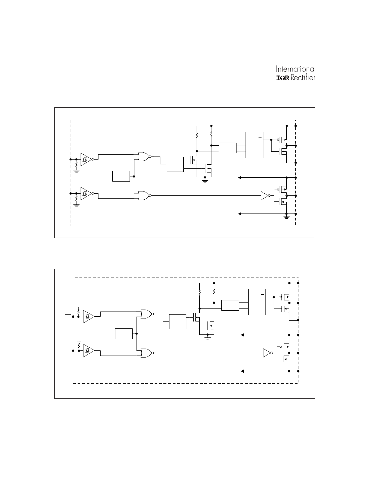
Functional Block Diagram
V
B
HIN
LIN
HIN
v
15V
v
15V
Q
R
S
HO
V
S
V
CC
LO
COM
UV
DETECT
PULSE
GEN
HV
LEVEL
SHIFT
PULSE
FILTER
IR2101/IR21014
V
B
HV
cc
PULSE
GEN
UV
cc
DETECT
LEVEL
SHIFT
PULSE
FILTER
Q
R
S
HO
V
S
V
CC
LIN
LO
COM
IR2102/IR21024
4
IR2101/IR21014/IR2102/IR21024
Lead Definitions
Symbol Description
HIN Logic input for high side gate driver output (HO), in phase (IR2101)
HIN Logic input for high side gate driver output (HO), out of phase (IR2102)
LIN Logic input for low side gate driver output (LO), in phase (IR2101)
LIN Logic input for low side gate driver output (LO), out of phase (IR2102)
V
B
HO High side gate drive output
V
S
V
CC
LO Low side gate drive output
COM Low side return
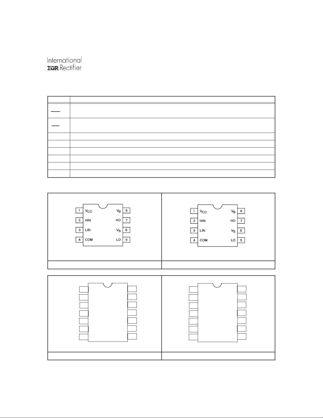
Lead Assignments IR2101
High side floating supply
High side floating supply return
Low side and logic fixed supply
8 Lead PDIP 8 Lead SOIC
IR2101 IR2101S
1
2
V
CC
3
HIN
4
LIN
5
COM
6
LO
7
14 Lead PDIP 14 Lead SOIC
V
HO
V
14
13
12
B
11
10
S
9
8
1
V
2
CC
HIN
3
LIN
4
COM
5
LO
6
7
IR21014 IR21014S
5
V
HO
V
14
13
12
B
11
10
S
9
8

IR2101/IR21014/IR2102/IR21024
Lead Assignments IR2102
8 Lead PDIP 8 Lead SOIC
IR2102 IR2102S
V
HO
V
14
13
12
B
11
10
S
9
8
1
2
V
CC
3
HIN
4
LIN
5
COM
6
LO
7
1
V
2
CC
HIN
3
LIN
4
COM
5
LO
6
7
14 Lead PDIP 14 Lead SOIC
IR21024 IR21024S
6
V
HO
V
14
13
12
B
11
10
S
9
8

IR2101/IR21014/IR2102/IR21024
8 Lead PDIP
01-3003 01
8 Lead SOIC
7
01-0021 08

IR2101/IR21014/IR2102/IR21024
14 Lead PDIP
14 Lead SOIC (narrow body)
01-3002 03
01-3063 00
8

HIN
LIN
IR2101/IR21014/IR2102/IR21024
HIN
LIN
50%
50%
HIN
LIN
HO
LO
Figure 1. Input/Output Timing Diagram
HIN
LIN
HIN
LIN
50%
50% 50%
50%
HIN
50%
50%
LIN
t
on
t
r
90% 90%
t
off
t
f
HO
LO
Figure 2. Switching Time Waveform Definitions
10% 10%
LO
MT
HO
10%
MT
90%
HOLO
Figure 3. Delay Matching Waveform Definitions
9

IR2101/IR21014/IR2102/IR21024
500
400
300
Max.
200
100
Turn-On Delay Time (ns)
Typ.
0
-50 -25 0 25 50 75 100 125
T emperature (°C)
500
400
.
Max
300
200
Typ.
100
Turn -On Delay Time (ns)
0
10 12 14 16 18 20
VBIAS Supply Voltage (V)
Figure 6A. Turn-On Time vs Voltage Figure 6B. Turn-On Time vs Voltage
500
400
300
Max .
200
100
Turn-Off Delay T ime (ns)
Ty p .
0
-50 -25 0 25 50 75 100 125
T emperature (°C)
500
400
Max.
300
200
Typ.
100
Turn-Off Delay T ime (ns)
0
10 12 14 16 18 20
VBIAS Supply Voltage (V)
Figure 7A. Turn-Off Time vs Temperature
500
400
300
200
Max
.
100
Turn-On Rise T ime (ns)
Ty p .
0
-50 -25 0 25 50 75 100 125
T emperature (°C)
Figure 7B. Turn-Off Time vs Voltage
500
400
300
Max .
200
100
Turn-On Rise T ime (ns)
Ty p .
0
10 12 14 16 18 20
VBIAS Supply Voltage (V)
Figure 9A. Turn-On Rise Time vs Temperature Figure 9B. Turn-On Rise Time vs Voltage
10

Turn-Off Fall T ime (ns)
IR2101/IR21014/IR2102/IR21024
200
150
100
Max
.
50
Turn-Off Fall T ime (ns)
Ty p .
0
-50 -25 0 25 50 75 100 125
T emperature (°C)
Figure 10A. Turn-Off Fall Time vs Temperature
8
7
6
5
4
Min.
3
2
Input Voltage (V )
1
0
-50 -25 0 25 50 75 100 125
T emperature (°C)
200
150
Max.
100
50
Ty p .
Turn-Off Fall T ime (ns)
0
10 12 14 16 18 20
VBIAS Supply Voltage (V)
Figure 10B. Turn-Off Fall Time vs Voltage
8
7
6
5
4
Min.
3
2
Input V oltage (V)
1
0
10 12 14 16 18 20
Vcc Supply Voltage (V)
Figure 12A. Logic "1" Input Voltage (IR2101)
Logic "0" Input Voltage (IR2102)
vs Temperature
4
3.2
2.4
1.6
Max
Input Voltage (V )
0.8
.
0
-50 -25 0 25 50 75 10 0 125
T emperature (°C) Vcc Supply Voltage (V)
Figure 13A. Logic "0" Input Voltage (IR2101)
Logic "1" Input Voltage (IR2102)
vs Temperature
Figure 12B. Logic "1" Input Voltage (IR2101)
Logic "0" Input Voltage (IR2102)
vs Voltage
4
3.2
2.4
1.6
Max
Input Voltage (V )
0.8
.
0
10 12 14 16 18 20
Figure 13B. Logic "0" Input Voltage (IR2101)
Logic "1" Input Voltage (IR2102)
vs Voltage
11

IR2101/IR21014/IR2102/IR21024
1
0.8
0.6
0.4
Max .
0.2
High Level Output Voltage (V)
0
-50 -25 0 25 50 75 100 125
T emperature (°C)
Figure 14A. High Level Output
vs Temperature
1
0.8
0.6
0.4
0.2
Max .
Low Level Output Voltage (V)
0
-50 -25 0 25 50 75 100 125
T emperature (°C)
1
0.8
0.6
0.4
Max.
0.2
High Level Output Voltage (V)
0
10 12 14 16 18 20
Vcc Supply Voltage (V)
Figure 14B. High Level Output vs Voltage
1
0.8
0.6
0.4
0.2
Max.
Low Level Output Voltage (V)
0
10 12 14 16 18 20
Vcc Supply Voltage (V)
Figure 15A. Low Level Output
vs Temperature
500
400
300
200
100
Max.
0
-50-25 0 25 50 75100125
Offset Supply Leakage Current (µA)
T emperature (°C)
Figure 16A. Offset Supply Current
vs Temperature
12
Figure 15B. Low level Output vs Voltage
500
400
300
200
100
Max.
0
0 100 200 300 400 500 600
Offset Supply Leakage Current (µA)
VB Boost Voltage (V)
Figure 16B. Offset Supply Current
vs Voltage

IR2101/IR21014/IR2102/IR21024
150
120
90
60
Max .
30
VBS Supply Current (µA)
Ty p .
0
-50 -25 0 25 50 75 10 0 125
T emperature (°C)
Figure 17A. VBS Supply Current
vs Temperature
700
600
500
400
Max .
300
200
Vcc Supply Current (µA)
100
Ty p .
0
-50 -25 0 25 50 75 100 125
T emperature (°C)
150
120
90
60
Max.
30
VBS Supply Current (µA)
Typ.
0
10 12 14 16 18 20
VBS Floating Supply Voltage (V)
Figure 17B. V
BS Supply Current
vs Voltage
700
600
500
400
300
Max .
200
Vcc Supply Current (µA)
100
Ty p .
0
10 12 14 16 18 20
Vcc Supply Voltage (V)
Figure 18A. Vcc Supply Current
vs Temperature
30
25
20
15
10
Max .
5
Logic 1” Input Current (µA)
Ty p .
0
-50-25 0 25 50 75100125
T emperature (°C)
Figure 19A. Logic"1" Input Current
vs Temperature
13
Figure 18B. Vcc Supply Current
vs Voltage
30
25
20
15
10
Max .
5
Ty p .
Logic 1” Input Current (µA)
0
10 12 14 16 18 20
Vcc Supply Voltage (V)
Figure 19B. Logic"1" Input Current
vs Voltage

IR2101/IR21014/IR2102/IR21024
5
4
3
2
Max.
1
Logic “0” Input Current (µA)
0
-50 -25 0 25 50 75 100 125
T emperature (°C)
Figure 20A. Logic "0" Input Current
vs Temperature
11
Max .
10
Typ .
9
Min .
8
7
VCC UVLO Threshold +(V)
6
-50-25 0 25 50 75100125
T emperature (°C)
5
4
3
2
Max.
1
Logic "0" Input Current (uA)
0
10 12 14 16 18 20
VCC Supply Voltage (V)
Figure 20B. Logic "0" Input Current
vs Voltage
11
10
Max.
9
Typ.
8
7
Min.
VCC UVLO Threshold - (V)
6
-50 -25 0 25 50 75 100 125
T emperature (°C)
Figure 21A. Vcc Undervoltage Threshold(+)
vs Temperature
500
400
Typ.
300
200
100
Min.
Output Source Current (mA)
0
-50 -25 0 25 50 75 100 125
T emperature (°C)
Figure 22A. Output Source Current
vs Temperature
Figure 21B. Vcc Undervoltage Threshold(-)
vs Temperature
500
400
300
200
Typ.
100
Output Source Current (mA)
Min.
0
10 12 14 16 18 20
VBIAS Supply Voltage (V)
Figure 22B. Output Source Current
vs Voltage
14

IR2101/IR21014/IR2102/IR21024
700
600
Typ .
500
400
300
Min.
200
100
Output Sink Current (mA)
0
-50-25 0 25 50 75100125
T emperature (°C)
Figure 23A. Output Sink Current
vs Temperature
700
600
500
400
Typ.
300
200
Min.
100
Output Sink Current (mA)
0
10 12 14 16 18 20
VBIAS Supply Voltage (V)
Figure 23B. Output Sink Current
vs Voltage
WORLD HEADQUARTERS: 233 Kansas St., El Segundo, California 90245 Tel: (310) 322 3331
IR GREAT BRITAIN: Hurst Green, Oxted, Surrey RH8 9BB, UK Tel: ++ 44 1883 732020
IR FAR EAST: K&H Bldg., 2F, 30-4 Nishi-Ikebukuro 3-Chome, Toshima-Ku, Tokyo, Japan 171 Tel: 81 3 3983 0086
IR SOUTHEAST ASIA: 1 Kim Seng Promenade, Great World City West Tower, 13-11, Singapore 237994 Tel: 65 221 8371
IR TAIWAN: 16 Fl. Suite D..207, Sec.2, Tun Haw South Road, Taipei, 10673, Taiwan Tel: 886-2-2377-9936
http://www.irf.com/ Data and specifications subject to change without notice. 3/22/99
IR CANADA: 15 Lincoln Court, Brampton, Ontario L6T 3Z2 Tel: (905) 453-2200
IR GERMANY: Saalburgstrasse 157, 61350 Bad Homburg Tel: ++ 49 6172 96590
IR ITALY: Via Liguria 49, 10071 Borgaro, Torino Tel: ++ 39 11 451 0111
15
 Loading...