查询IR2086S供应商
HIGH SPEED, 100V, SELF OSCILLATING 50% DUTY CYCLE,
Data Sheet PD No.60226
IR2086S
FULL-BRIDGE DRIVER
Features
Simple primary side control solution to enable full-bridge
•
DC-Bus Converters for 48V distributed systems with reduced
component count and board space.
Frequency and dead time set by two external components
•
Maximum 500KHz per channel output with 50% duty cycle
•
Adjustable dead time 50nsec ~ 200nsec
•
Floating channel designed for bootstrap operation up to +100Vdc
•
High and low side pulse width matching to +/- 25nsec
•
Overcurrent protection with adjustable hiccup period.
•
Undervoltage lockout and internal soft start
•
Product Summary
V
CC (max)
V
offset(max)
High/low side
output freq (f
Output Current (I
High/low side pulse
edge matching +/- 25ns
Description
The IR2086S is a self oscillating full-bridge controller and driver IC with
50% duty cycle ideally suited for 36V-75V full-bridge DC Bus Converters.
Dead time can be controlled through proper selection of C
from 50 to 200nsec. Internal soft start increases pulse width on power up
and maintains equal pulse widths for the high and low outputs throughout
the start up cycle. Undervoltage lockout prevents operation if Vcc is less than
7.5 Vdc. Over current shutdown occurs when the voltage on the Cs pin
exceeds 200mV. Restart after overcurrent trip can be delayed by adjusting
the external capacitor. The delay time ranges from 10µs to 1s.
Typical
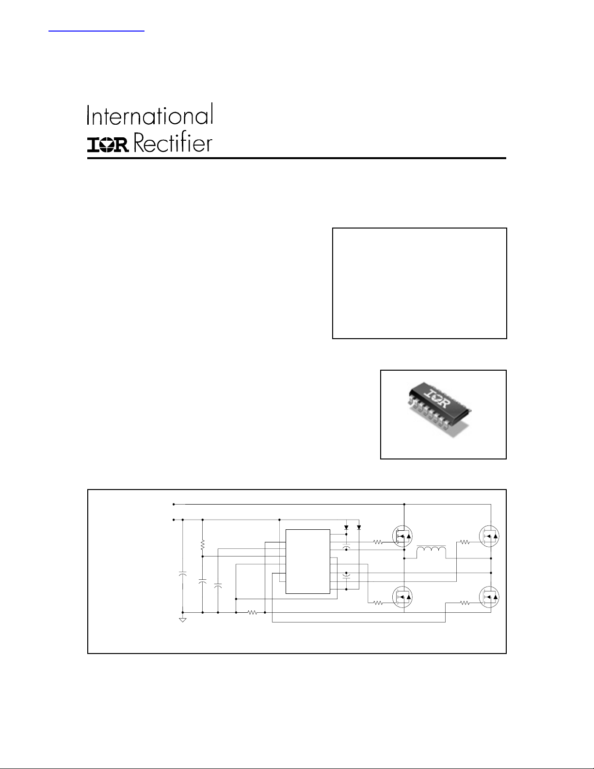
Connection
(Refer to Lead Assignments for correct pin
configuration). This/
These diagram(s)
show electrical connections only. Please refer
to our Application
Notes and DesignTips
for proper circuit board
layout.
VBUSS (100 VDC MAX)
VCC (9 ~15V)
RT
CT
*COM2 must be shorted to COM1 for proper operation
**CD is optiona l
CD**
RSENSE
and can range
T
IR2086S
CS
DELAY
CT
COM2*
COM1
LO1
VCC
VB1
HO1
VS1
LO2
VS2
HO2
VB2
25V
100Vdc
) 500kHz
osc
) +/-1.2A
O
Package
16-Lead SOIC

IR2086S
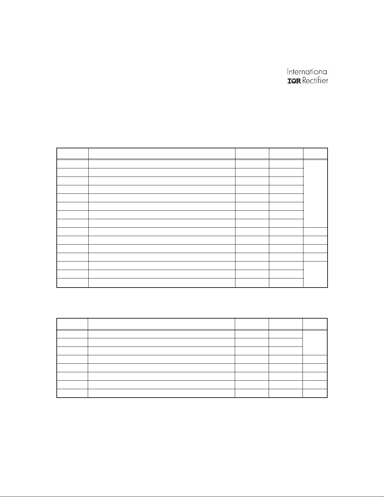
Absolute Maximum Ratings
V
(VCC, VBS) = 12V, CL = 1000 pF, and TA = 25°C unless otherwise specified.
BIAS
Absolute maximum ratings indicate sustained limits beyond which damage to the device may occur. All voltage parameters
are absolute voltages referenced to COM. All currents are defined positive into any lead. The thermal resistance and power
dissipation ratings are measured under board mounted and still air conditions.
Symbol Definition Min. Max. Units
V
CC
V
B1,2
V
S1,2
V
HO1,2
V
LO1,2
V
CT
V
CS
V
DELAY
dVS/dt Allowable offset voltage slew rate -50 +50 V/ns
I
CC
P
D
Rth
JA
T
J
T
S
T
L
Low side supply voltage -0.3 25
High side floating supply voltage -0.3 150
High side floating supply offset voltage V
High side floating output voltage V
Low side output voltage -0.3 VCC + 0.3
CT pin voltage -0.3 VCC + 0.3
Cs pin voltage -0.3 VCC + 0.3
Delay pin voltage -0.3 VCC + 0.3
Supply current — 40 mA
Package power dissipation
Thermal resistance, junction to ambient (16-lead SOIC) — 200 °C/W
Junction temperature -55 150
Storage temperature -55 150
Lead temperature (soldering, 10 seconds) — 300
(16-lead SOIC) — 1.0
- 25 V
B1,2
- 0.3 V
B1,2
B1,2
B1,2
+ 0.3
+ 0.3
Vdc
W
°C
Recommended Operating Conditions
For proper operation the device should be used within the recommended conditions.
Symbol Definition Min. Max. Units
V
B1,2
V
S1,2
V
CC
I
CC
R
T
C
T
fmax Operating frequency (per channel) — 500
T
j
Note1: Care should be taken to avoid output switching conditions where the Vs node flies inductively below ground by
more than 5V.
High side floating supply voltage
Steady state high side floating supply offset voltage -5 100
Supply voltage 9.5 15
Supply current — 1 mA
Timing resistor 10 100 Kohms
Timing capacitor 47 1000 pF
Junction temperature -40 125 °C
2
9.5 15
Vdc
KHz
www.irf.com

IR2086S
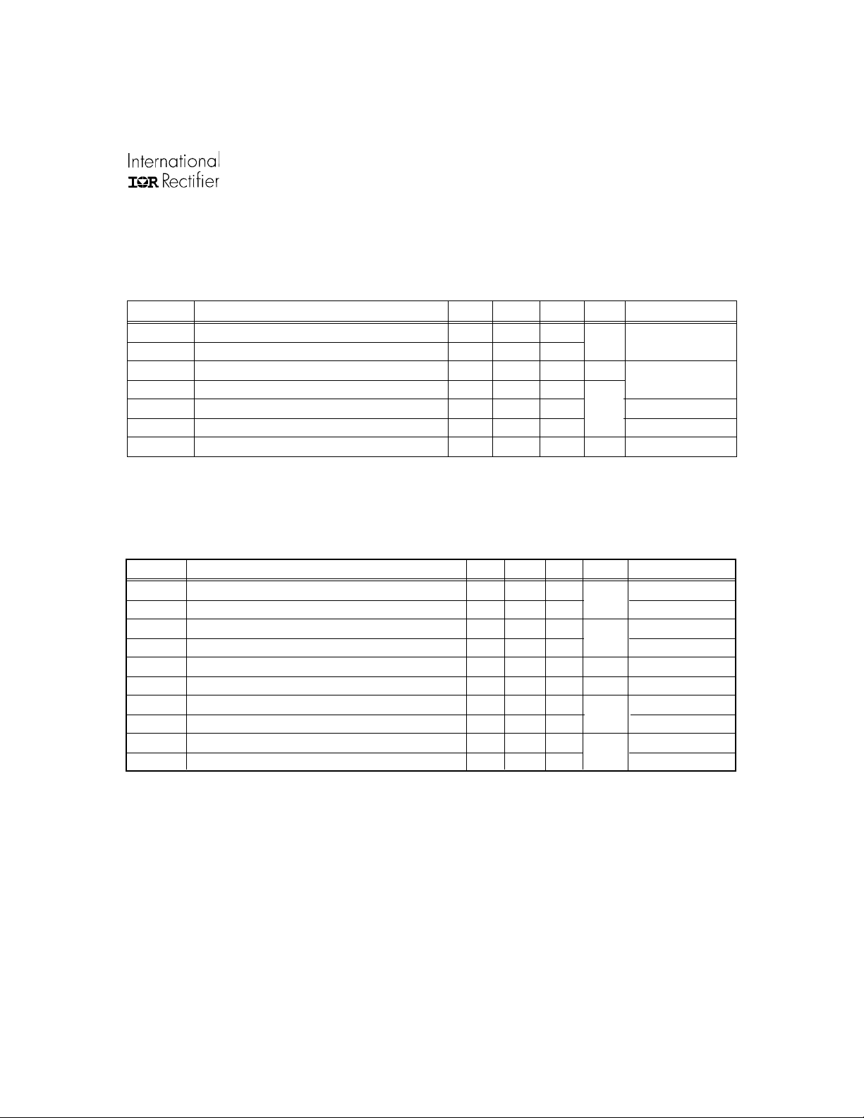
Dynamic Electrical Characteristics
V
(VCC, VBS) = 12V, CL = 1000 pF, and TA = 25°C unless otherwise specified.
BIAS
Symbol Definition Min. Typ. Max. Units Test Conditions
t
t
fout Per channel output frequency 450 500 550 KHz
tdt High/low output dead time 50 — —
PM High/low pulse width matching — 25 — VS = 0V ~ 100V
t
dcs
t
restart
Static Electrical Characteristics
V
BIAS
Symbol Definition Min. Typ. Max. Units Test Conditions
V
OH1,2
V
OL1,2
I
leak
I
QBS
I
QCC
V
CS+ Overcurrent shutdown threshold
U
VCC+
U
VCC-
I
O+
I
O-
Turn-on rise time — 40 60
r
Turn-off fall time — 20 30
f
Overcurrent shut down delay — 200 —
Overcurrent restart delay — 0.5 — sec Vcc =15V, Cd=100nF
(VCC, VBS) = 12V, CL = 1000 pF and TA = 25°C unless otherwise specified.
High level output voltage, (V
Low level output voltage — — 0.1
Offset supply leakage current — — 50
Quiescent VBS supply current — — 150
Quiescent VCC supply current — — 1.75 mA
Undervoltage positive going threshold 6.5 7.25 8.0
Undervoltage negative going threshold 6.0 6.8 7.7
Output high short circuit current — 1.2 —
Output low short circuit current — 1.2 —
- VO) — — 1.5
BIAS
— 300 — mV
nsec
nsec
V
µA
V
A
VS = 0V
Ct=100pF,
Rt=10Kohm
www.irf.com
3
 Loading...