

查询IR20153S供应商
Preliminary Data Sheet PD60214 Rev B
IR20153S & (PbF)
HIGH SIDE DRIVER WITH RECHARGE
Features
Product Summary
• Floating channel designed for bootstrap operation
Fully operational up to 150V
Tolerant to negative transient voltage, dV/dt immune
• Gate drive supply range from 5V to 20V
• Undervoltage lockout
V
OFFSET
IO+/- 400mA @ VBS=7V,
• Internal recharge FET for bootstrap refresh
• Internal deadtime of 11µs and 0.8µs
• CMOS Schmitt-triggered input logic
• Output out of phase with input
• Reset input
• Split pull-up and pull-down gate drive pins
V
OUT
t
on/off
• Also available LEAD-FREE (PbF)
Description
The IR20153S is a high voltage, high speed power MOSFET driver . Proprietary HVIC
and latch immune CMOS technologies enable ruggedized monolithic construction. The
logic input is compatible with standard CMOS output down to 3.3V. The output driver
features a high pulse current buffer stage designed for minimum cross-conduction. The
floating channel can be used to drive an N-channel power MOSFET in the high or low
side configuration which operates up to 150 volts.
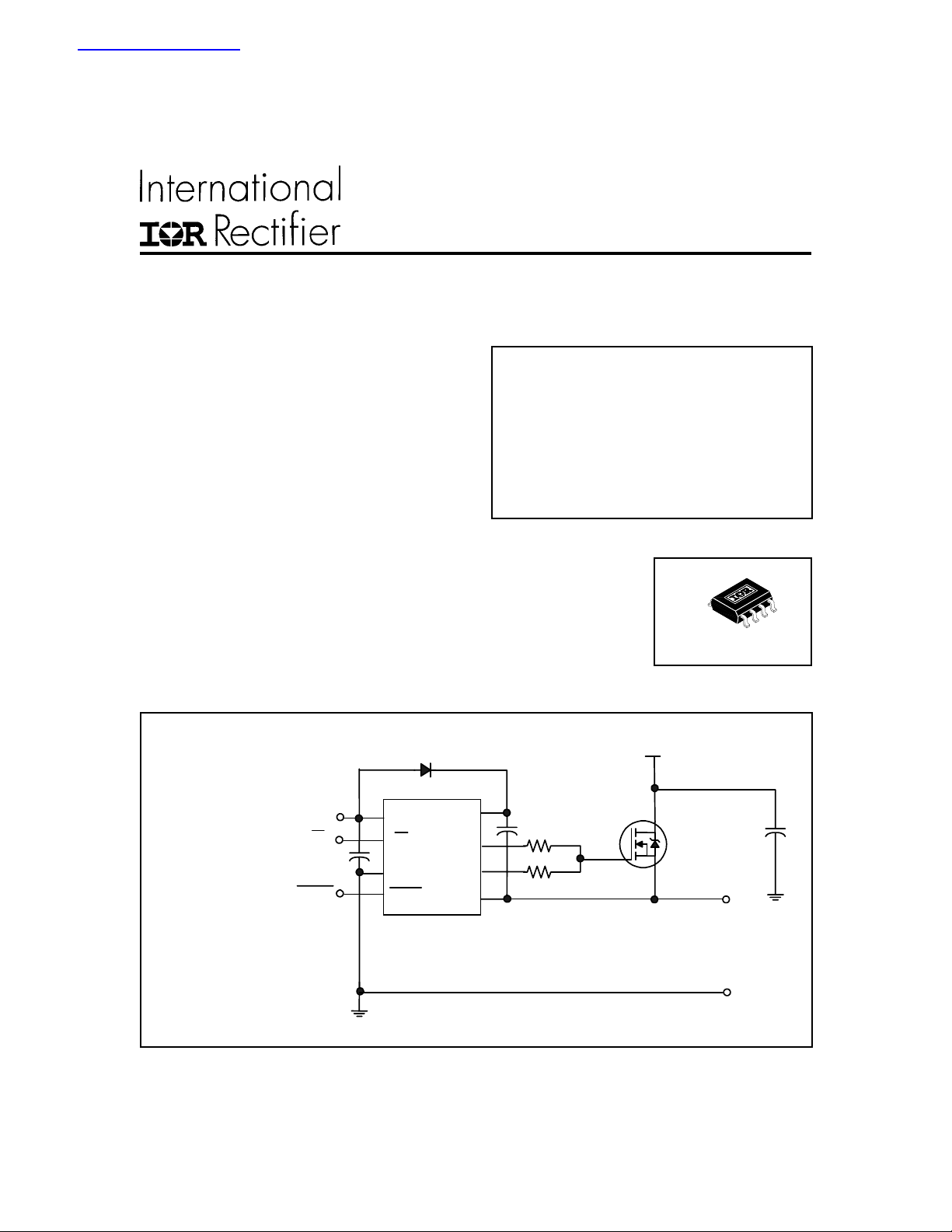
Typical Connection
150V max.
1.5A @ VBS=16V
5-20V
1.0 and 0.3 µs
Package
8-Lead SOIC
up to 150V
VCC
IN
RESET
(Refer to Lead Assignments
for correct configuration).
This/These diagram(s) show
electrical connections only.
Please refer to our Application Notes and DesignTips
for proper circuit board layout.
www.irf.com 1
VCC
IN
GND
RESET
VB
HOH
HOL
VS
Load
IR20153S & (PbF)
Absolute Maximum Ratings
Absolute maximum ratings indicate sustained limits beyond which damage to the device may occur. All voltage parameters are absolute voltages referenced to GND, all currents are defined positive into any lead. This is a stress only rating
and operation of the device at these or any conditions exceeding those indicated in the operational sections of this
specifications is not implied.
Symbol Definition Min. Max. Units
V
B
V
S
V
HO
V
CC
V
IN
dV/dt Allowable offset voltage slew rate — 50 V/nsec
T
J
T
S
T
L
High side driver output stage voltage -5.0 170
High side floating supply offset voltage - 8.0 150
Output voltage gate high connection VS - 0.3 V
Low side fixed supply voltage -0.3 25
Input voltage (IN and RESET) -0.3 V
Junction temperature -55 150
Storage temperature -55 150
Lead temperature (soldering, 10 seconds) — 300
B
+ 0.3
CC
°C
V
+0.3
Recommended Operating Conditions
The input/output logic timing diagram is shown in Fig. 2. For proper operation the device should be used within the
recommended conditions. All voltage parameters are absolute voltages referenced to GND. The VS offset rating is tested
with all suppliers biased at Vcc=5V and VBS=7V.
Symbol Definition Min. Max. Units
V
B
V
S
V
HO
V
CC
V
IN
T
A
2 www.irf.com
High side driver output stage voltage VS + 5 VS + 20
High side floating supply offset voltage -1.6 150
Output voltage gate high connection V
Supply voltage 5 20
Input voltage (IN and RESET) 0 Vcc
Ambient temperature -55 150 °C
S
V
B
V
IR20153S & (PbF)
Electrical Characteristics
Unless otherwise specified,
Unless otherwise noted, these specifications apply for an operating ambient temperature of TA =25°C.
Symbol Definition Min. Typ. Max. Units Test Conditions
VCC Supply Characteristics
V
CCUV+
V
CCUV-
V
CCUVHYSVCC
I
QCC
VBS Supply Characteristics
V
BSUV
V
BSUV
V
BSUVHYSVBS
I
QBS1
I
QBS2
VB. VS Supply Characteristics
I
LK
Gate Driver Characteristics
I
o+1
I
o+2
t
r1
t
r2
I
o-1
I
o-2
t
f1
t
f2
t
on
t
off
t
res,off
VCC supply undervoltage positive going threshold
VCC supply undervoltage negative going threshold 2.5 — — VCC dropping
VCC supply current
+VBS supply undervoltage positive going threshold
-VBS supply undervoltage negative going threshold 2.5
VBS supply current
VBS supply current
Offset supply leakage current
Peak output source current 250 400
Peak output source current 800 1500
Output rise time
Output rise time
Peak output sink current 250 400
Peak output sink current 800 1500
Output fall time
Output fall time
Input-to-Output Turn-on propogation delay
(50% input level to 10% output level)
Input-to-Output Turn-off propogation delay
(50% input level to 90% output level)
RES-to-Output Turn-off propogation delay
(50% input level to 90% [t
VCC = 5V, VBS = 7V, VS = 0V, IN = 0V, RES = 5V, load R = 50Ω, C = 6.8nF (see Figure 3).
——
supply undervoltage lockout hysteresis 0.01 0.3 0.60
——
——
supply undervoltage lockout hysteresis 0.01 0.3 0.60
——
——
——
—
—
—
—
—
—
—
] output levels)
phl
4.3
400 uA VCC = 3.6V & 6.5V
4.3 V VBS rising from 0V
——
100
200
50
—
—
0.2 0.4µsec
0.1 0.2µsec VBS = 16V
—
—
0.2 0.4µsec IN = 5V
0.1 0.2µsec VBS = 16V, IN = 5V
1.0 2.0µsec
0.3 0.9µsec
0.3 0.9µsec
V
V
µ
A static mode, VBS =
µ
A static mode, VBS =
16V, IN = 0V or 5V
µ
AVB = VS = 150V
mA
mA VBS = 16V
mA IN = 5V
mA VBS = 16V, IN = 5V
rising from 0V
CC
from 5V
VBS dropping
from 5V
7V, IN = 0V or 5V
www.irf.com 3
IR20153S & (PbF)
Electrical Characteristics
Unless otherwise specified,
Unless otherwise noted, these specifications apply for an operating ambient temperature of T
VCC = 5V, VBS = 7V, VS = 0V, IN = 0V, RES = 5V, load R = 50
Symbol Definition Min. Typ. Max. Units Test Conditions
Gate Driver Characteristics cont.
Supply Characteristics
V
CC
t
res,on
RES-to-Output Turn-On Propogation Delay - 1.0 2.0
(50% input level to 10% [t
] output levels)
plh
Input Characteristics
V
INH
V
INL
R
IN
V
H_RES
V
L_RES
R
RES
Recharge Characteristics
t
on_rech
t
off_rech
V
RECH
High Logic Level Input Threshold 3 - - V
Low Logic Level Input Threshold - - 1.4 V
High Logic Level Input Resistance 40 100 220 k
High Logic Level RES Input Threshold 3 - - V
Low Logic Level RES Input Threshold - - 1.4 V
High Logic Level RES Input Resistance 40 100 220 k
(see Figure 3a)
Recharge Transistor Turn-On Propogation Delay 7 11 15
Recharge Transistor Turn-Off Propogation Delay - 0.3 0.9
Recharge Output Transistor On-State Voltage Drop - - 1.2 V IS = 1mA, IN = 5V
Deadtime Characteristics
DT
DT
HOFF
HON
High Side Turn-Off to Recharge gate Turn-On 7 11 15
Recharge gate Turn-Off to High Side Turn-On0. 0.4 0.8 1.5
Ω
, C = 6.8nF (see Figure 3).
=25°C.
A
µ
sec
Ω
Ω
µ
sec VS = 5V
µ
sec
µ
sec
µ
sec
4 www.irf.com
IR20153S & (PbF)
A True table for
,
V
cc
, RESET, IN,
V
BS
LOW IN.
V
cc VBS
<V
ccUVLO-
<V
ccUVLO-
<V
ccUVLO-
<V
ccUVLO-
<V
ccUVLO-
<V
ccUVLO-
<V
ccUVLO-
<V
ccUVLO-
>V
ccUVLO+
>V
ccUVLO+
>V
ccUVLO+
<VBSUVLO-
<VBSUVLO-
<VBSUVLO-
<VBSUVLO-
>VBSUVLO+
>VBSUVLO+
>VBSUVLO+
>VBSUVLO+
<VBSUVLO-
<VBSUVLO-
<VBSUVLO-
and RechFET is shown as follows.
H
O
RESET- IN-
HIGH HIGH OFF ON
HIGH LOW OFF ON
LOW HIGH OFF ON
LOW LOW OFF ON
HIGH HIGH OFF ON
HIGH LOW OFF ON
LOW HIGH OFF ON
LOW LOW OFF ON
HIGH HIGH OFF ON
HIGH LOW OFF OFF
LOW HIGH OFF ON
This truth table is for ACTIVE
H
O
RechFET
>V
ccUVLO+
>V
ccUVLO+
>V
ccUVLO+
>V
ccUVLO+
>V
ccUVLO+
RESET = HIGH indicates that high side MOSFET is allowed to be turned on.
<VBSUVLO-
>VBSUVLO+
>VBSUVLO+
>VBSUVLO+ LOW HIGH OFF ON1
>VBSUVLO+
LOW LOW OFF ON
HIGH HIGH OFF ON
HIGH LOW ON OFF
LOW LOW OFF ON
1
1
1
RESET = LOW indicates that high side MOSFET is OFF.
IN = LOW indicates that high side MOSFET is on.
IN = HIGH indicates that high side MOSFET is off.
RechFET = ON indicates that the recharge MOSFET is on.
RechFET = OFF indicates that the recharge MOSFET is off.
1
Note: Refer to the RESET functionality graph of Figure 7, for VCC and VBS voltage ranges under which
the functionality is normal.
www.irf.com 5

IR20153S & (PbF)
Functional Block Diagram
VCC
UV
DETECT
RESET
LOGIC
IN
PULSE
GEN
DELAYS
HV
LEVEL
SHIFT
UV
DETECT
PULSE
FILTER
RSQ
R
RECHARGE
SWITCH
VB
HOH
HOL
VS
Lead Definitions and Assignments
Symbol Description
V
CC
I IN- Driver Control Signal Input
GND Ground
RESET Driver Enable Signal Input
V
S
H
OL
H
OH
V
B
6 www.irf.com
Driver Supply
MOSFET Source Connection
MOSFET Gate Low Connection
MOSFET Gate High Connection
Driver Output Stage Supply
1
VCC
2
IN-
3
GND
4
RESET-
8-Lead SOIC
HOH
HOL
VB
VS
8
7
6
5

IN-
RESET-
HO-VS
IR20153S & (PbF)
Figure 1. Input/Output Functional Diagram
IN
RES
HOH,L
res,on
T
Figure 1a. Reset Timing Diagram
www.irf.com 7
T
res,off

IR20153S & (PbF)
IN
RESET
Vs
HOH,L
Recharge
FET
T
on
OFF ON
T
off_rech
Figure 2. Input/Output Timing Diagram
90%
T
off
T
on_rech
90%
5V
10%
T
r
Figure 2a. Output Timing Diagram
8 www.irf.com
T
10%
f

IR20153S & (PbF)
V
V
5V
CC VB
IN- HOH
GND HOL
RESET- VS
7V
50ohm
50ohm
6.8nF
Figure 3. Switching Time Test Circuit
5V
CC VB
7V
50ohm
IN- HOH
GND HOL
RESET- VS
50ohm
5V
6.8nF
Figure 3a. Ton_rech and Toff_rech Test Circuit
www.irf.com 9

IR20153S & (PbF)
)
3.4
3.2
3
2.8
Vinth+ (V)
2.6
2.4
2.2
4.4 4.7 5 5.3 5.6 5.9 6.2 6.5
Vs upply (V)
Figure 4. Positive Input and Reset
Threshold Voltage vs. Vsupply
160
140
2.8
2.5
2.2
1.9
VINth- (V)
1.6
1.3
4.4 4.7 5 5.3 5.6 5.9 6.2 6.5
Vsupply (V)
Figure 5. Negative Input and Rese t
Thres hold Voltage vs. Vsupply
2.2
1.9
120
100
RIN (kohm
80
60
40
-50-25 0 25 50 75100125
Figure 6. Input and Reset Impedance
vs. Temperature
T (
o
C )
1.6
1.3
I (mA)
1
0.7
0.4
0.6 0.8 1 1.2 1.4
V (V)
Figure 7. Recharge FET I-V Curve
10 www.irf.com

IR20153S & (PbF)
)
)
35
30
125oC 25oC
-40oC
25
20
15
VBS (V)
10
5
0
3.4 3.8 4.2 4.6 5
V CC ( V )
Figure 8. Reset Functionality
This graph explains the functionality limitation as a
function of VCC, VBS and temperature. Each curve on
the graph represents VCC Vs. VBS, for a particular
temperature. For each particular temperature and VCC,
the output is non-functional for any value of VBS above
the drawn curve. But for any value of VBS below the
curve the functionality is fine.
700
2200
1800
- 40C
1400
1000
125C
600
Output Sink Current (mA
200
5101520
VBS (V)
Figure 9. Output Sink Current
vs. VBS
1300
650
600
1200
1100
550
1000
500
450
Output Source Current (mA)
400
-50 0 50 100 150
Temperature (
o
C)
Figure 10. Output Source Curre nt
www.irf.com 11
vs. Temperature , VBS=7V
900
Turn-on Propagation Delay (ns
800
-50 0 50 100 150
o
Temperature (
C)
Figure 11. Turn-on Propagation De lay
vs. Temperature , VBS=7V

IR20153S & (PbF)
y
n
320
280
240
Turn-off Propagation Delay (ns)
200
-50 0 50 100 150
Temperature (
o
C)
Figure 12. Turn-off Propagation Delay
vs. Te m per ature, VBS=7V
350
300
250
200
Delay (ns)
150
1300
1200
1100
1000
(ns)
900
800
-50 0 50 100 150
o
RES-to-Output Turn-on Propagation Dela
Temperature (
C)
Figure 13. RES-to-Output Turn-on Propagation
Delay vs . Tem per ature, VBS=7V
200
175
150
125
100
100
50
RES-to-Output Turn-off Propagatio
-50 0 50 100 150
Temperature (
o
C)
Figure 14. RES-to-Output Turn-off Propagation
Delay vs . Tem per ature, VBS=7V
75
50
-50 0 50 100 150
High Logic Level Input Resistance (kohm
Temperature (
o
C)
Figure 15. High Logic Level Input Resistance
vs. Te m per ature, VBS=7V
12 www.irf.com

IR20153S & (PbF)
e
n
n
175
150
125
100
(kohm)
75
50
High Logic Level RES Input Resistanc
-50 0 50 100 150
o
Temperature (
C)
Figur e 16. High Logic L evel RES Input Res is tance
vs. Temperature , VBS=7V
320
300
12
11
10
Delay (us)
9
8
-50 0 50 100 150
Recharge Transistor Turn-on Propagatio
Temperature (
o
C)
Figure 17. Recharge Transistor Turn-on
Propagation Delay vs. Tempe rature, VBS=7V
11
10.5
280
260
240
Delay (ns)
220
200
-50 0 50 100 150
Recharge Transistor Turn-off Propagation
Figure 18. Recharge Transistor Turn-off
Temperature (
o
C)
Propagation Delay vs . Tempe rature , V BS=7V
10
9.5
9
on (us)
8.5
8
-50 0 50 100 150
High Side Turn-off to Recharge Gate Tur
Temperature (
o
C)
Figure 19. High Side Turn-off to Recharge Gate
Turn-on vs. Tem perature, VBS=7V
www.irf.com 13

IR20153S & (PbF)
n
1200
1000
800
on (ns)
600
400
Recharge Gate Turn-off to High Side Tur
Figure 20. Re charge Gate Turn-off to High Side
Turn-on vs. Tem perature, VBS=7V
Case outline
-50 0 50 100 150
o
Temperature (
C)
.0688
.0098
.020
.1968
.1574
.2440
.0196
.050
8°
MILLIMETERSIN C H E S
MIN MAX
1.35
1.75
0.10
0.25
0.33
0.51
4.80
5.00
3.80
4.00
1.27 BAS IC
5.80
6.20
0.25
0.50
0.40
1.27
0°
8°
01-6027
(MS-012AA)
D B
FOOTPRINT
8X 0.72 [.028]
8X 1.78 [.070]
K x 45°
8X L
8X c
7
5 DIMENSION DOES NOT INCLUDE MOLD PROTRUSIONS.
MOL D PR OTRU SIONS N OT TO E XCE ED 0.15 [.006].
6 DIMENSION DOES NOT INCLUDE MOLD PROTRUSIONS.
MOL D PR OTRU SIONS N OT TO E XCE ED 0.25 [.010].
7 DIMENSION IS THE LENGTH OF LEAD FOR SOLDERING TO
A SU BSTRA TE.
8X b
5
65
4312
e1
A1
CAB
H
0.25 [.010] A
A
C
0.10 [.004]
6.46 [.255]
3X 1.27 [.050]
y
A
87
6
E
e
6X
0.25 [.010]
NOTES:
1. DIMENS IONING & TOL ERANC ING PER AS ME Y14.5M-1994.
2. CONTROLLING DIMENSION: MILLIMETER
3. DIMENSIONS ARE SHOWN IN MILLIMETERS [INC HES].
4. OUTLINE C ONFORMS TO JEDEC OUTLINE MS-012AA.
8-Lead SOIC
DIM
MIN MAX
.0532
A
.0040
A1
b
.013
c .0075 .0098 0.19 0.25
D
.189
E
.1497
e
.050 BAS IC
e1
.025 BA SIC 0.635 BA SIC
.2284
H
.0099
K
.016
L
y
0°
01-0021 11
14 www.irf.com

IR20153S & (PbF)
LEADFREE PART MARKING INFORMATION
Part number
Date code
Pin 1
Identifier
?
MARKING CODE
Lead Free Released
P
Non-Lead Free
Released
IRxxxxxx
YWW?
ORDER INFORMATION
Basic Part (Non-Lead Free)
8-Lead SOIC IR20153S order IR20153S
IR logo
?XXXX
Lot Code
(Prod mode - 4 digit SPN code)
Assembly site code
Per SCOP 200-002
Leadfree Part
8-Lead SOIC IR20153S order IR20153SPbF
Thisproduct has been designed and qualified for the industrial market.
Qualification Standards can be found on IR’s Web Site http://www.irf.com
IR WORLD HEADQUARTERS: 233 Kansas St., El Segundo, California 90245 Tel: (310) 252-7105
www.irf.com 15
Data and specifications subject to change without notice.
10/25/2004
 Loading...