

查询IR2011供应商
Data Sheet No.PD60217 Rev A
IR2011(
HIGH AND LOW SIDE DRIVER
Features
• Floating channel designed for bootstrap operation
Fully operational up to +200V
Tolerant to negative transient voltage, dV/dt immune
• Gate drive supply range from 10V to 20V
• Independent low and high side channels
• Input logicHIN/LIN active high
• Undervoltage lockout for both channels
• 3.3V and 5V input logic compatible
• CMOS Schmitt-triggered inputs with pull-down
• Matched propagation delay for both channels
• 8-Lead SOIC is also available LEAD-FREE (PbF)
Applications
• Audio Class D amplifiers
• High power DC-DC SMPS converters
• Other high frequency applications
Description
The IR2011 is a high power, high speed power MOSFET driver with independent high
and low side referenced output channels, ideal for Audio Class D and DC-DC converter
applications. L ogic inputs are compatible with standard CMOS or LSTTL output, down
to 3.0V logic. The output drivers feature a high pulse current buffer stage designed for
minimum driver cross-conduction. Propagation delays are matched to simplify use in
high frequency applications. The floating channel can be used to drive an N-channel
power MOSFET in the high side configuration which operates up to 200 volts. Proprietary HVIC and latch immune CMOS technologies enable ruggedized monolithic construction.
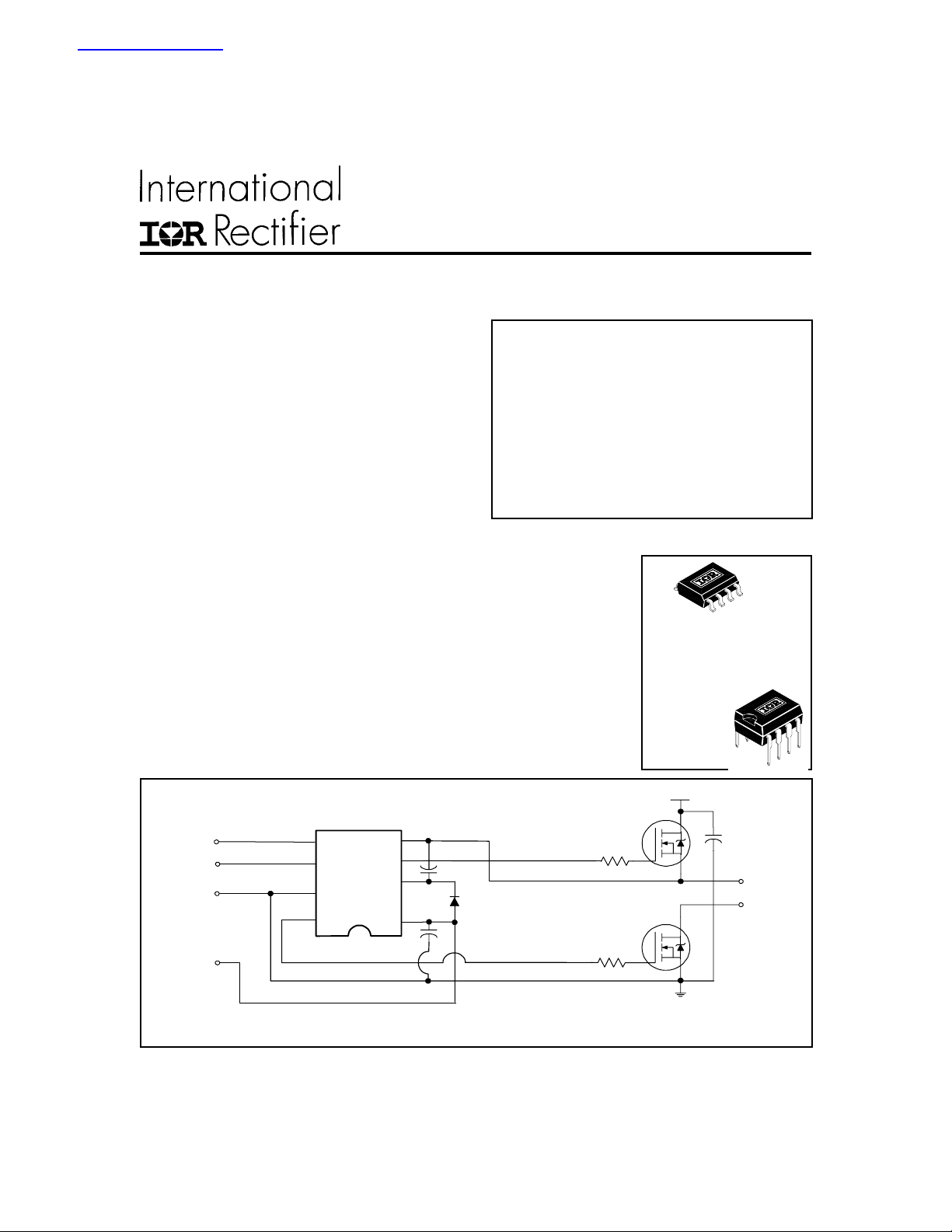
Typical Connection
Product Summary
V
OFFSET
IO+/- 1.0A /1.0A typ.
V
OUT
t
on/off
Delay Matching 20 ns max.
S) & (PbF
200V max.
10 - 20V
80 & 60 ns typ.
Packages
8-Lead SOIC
IR2011S
also available
LEAD-FREE (PbF)
8-Lead PDIP
IR2011
200V
)
45
V
V
HO
V
CC
S
B
18
TO
LOAD
HIN
LIN
COM
V
CC
(Refer to L ead Assignments for correct configuration). This/These diagram(s) show electrical connections only. Please
refer to our Application Notes and DesignTips for proper circuit board layout.
www.irf.com 1
HIN
LIN
COM
LO
IR2011(S) & (PbF)
Absolute Maximum Ratings
Absolute maximum ratings indicate sustained limits beyond which damage to the device may occur. All voltage parameters are absolute voltages referenced to COM. The thermal resistance and power dissipation ratings are measured
under board mounted and still air conditions.
Symbol Definition Min. Max. Units
V
B
V
S
V
HO
V
CC
V
LO
V
IN
dVs/dt Allowable offset supply voltage transient (figure 2) — 50 V/ns
P
D
R
THJA
T
J
T
S
T
L
High side floating supply voltage -0.3 250
High side floating supply offset voltage VB - 25 VB + 0.3
High side floating output voltage VS - 0.3 V
Low side fixed supply voltage -0.3 25
Low side output voltage -0.3 VCC +0.3
Logic input voltage (HIN & LIN) COM -0.3 V
Package power dissipation @ TA ≤ +25°C (8-lead DIP) — 1.0
(8-lead SOIC) — 0.625
Thermal resistance, junction to ambient (8-lead DIP) — 125
(8-lead SOIC) — 200
Junction temperature — 150
Storage temperature -55 150
Lead temperature (soldering, 10 seconds) — 300
B
CC
+ 0.3
+0.3
°C/W
°C
V
W
Recommended Operating Conditions
For proper operation the device should be used within the recommended conditions. The VS and COM offset ratings
are tested with all supplies biased at 15V differential.
Symbol Definition Min. Max. Units
V
B
V
S
V
HO
V
CC
V
LO
V
IN
T
A
Note 1: Logic operational for VS of -4 to +200V. Logic state held for VS of -4V to -VBS.
2 www.irf.com
High side floating supply absolute voltage VS + 10 VS + 20
High side floating supply offset voltage Note 1 200
High side floating output voltage V
Low side fixed supply voltage 10 20
Low side output voltage 0 VCC
Logic input voltage (HIN & LIN) COM 5.5
Ambient temperature -40 125 °C
S
V
B
V
IR2011(S) & (PbF)
Dynamic Electrical Characteristics
V
(VCC, VBS) = 15V, CL = 1000 pF, T
BIAS
Symbol Definition Min. Typ. Max. Units Test Conditions
t
t
DM1 Turn-on delay matching | t
DM2 Turn-off delay matching | t
on
off
Turn-on propagation delay — 80 — VS = 0V
Turn-off propagation delay — 75 — VS = 200V
t
Turn-on rise time — 35 5 0
r
t
Turn-off fall time — 20 35
f
Static Electrical Characteristics
V
(VCC, VBS) = 15V, and T
BIAS
COM and are applicable to all logic input leads: HIN and LIN. The VO and IO parameters are referenced to COM and are
applicable to the respective output leads: HO or LO.
= 25°C unless otherwise specified. The VIN, VTH and IIN parameters are referenced to
A
= 25°C unless otherwise specified. Figure 1 shows the timing definitions.
A
ns
(H) - t
on
off
(H) - t
(L) | — 5 20
on
(L) | — 5 20
off
Symbol Definition Min. Typ. Max. Units Test Conditions
V
IH
V
V
OH
V
OL
I
LK
I
QBS
I
QCC
I
IN+
I
IN-
V
BSUV+
V
BSUV-
V
CCUV+
V
CCUV-
I
O+
I
O-
www.irf.com 3
Logic “1” input voltage 2.2 — —
Logic “0” input voltage — — 0.7
IL
High level output voltage, V
Low level output voltage, V
BIAS
O
- V
O
— — 2.0 IO = 0A
— — 0.2 20mA
V
Offset supply leakage current — — 50 VB=VS = 200V
Quiescent VBS supply current — 90 210 V
Quiescent VCC supply current — 140 230 VIN = 0V or 3.3V
µA
Logic “1” input bias current — 7.0 20 VIN = 3.3V
Logic “0” input bias current — — 1.0 V
VBS supply undervoltage positive going 8.2 9 .0 9.8
threshold
VBS supply undervoltage negative going 7.4 8.2 9.0
threshold
V
VCC supply undervoltage positive going 8.2 9. 0 9.8
threshold
VCC supply undervoltage negative going 7.4 8 .2 9.0
threshold
Output high short circuit pulsed current — 1.0 — VO = 0V,
Output low short circuit pulsed current — 1.0 — VO = 15V,
A
VCC = 10V - 20V
= 0V or 3.3V
IN
= 0V
IN
PW ≤ 10 µs
PW ≤ 10 µs
IR2011(S) & (PbF)
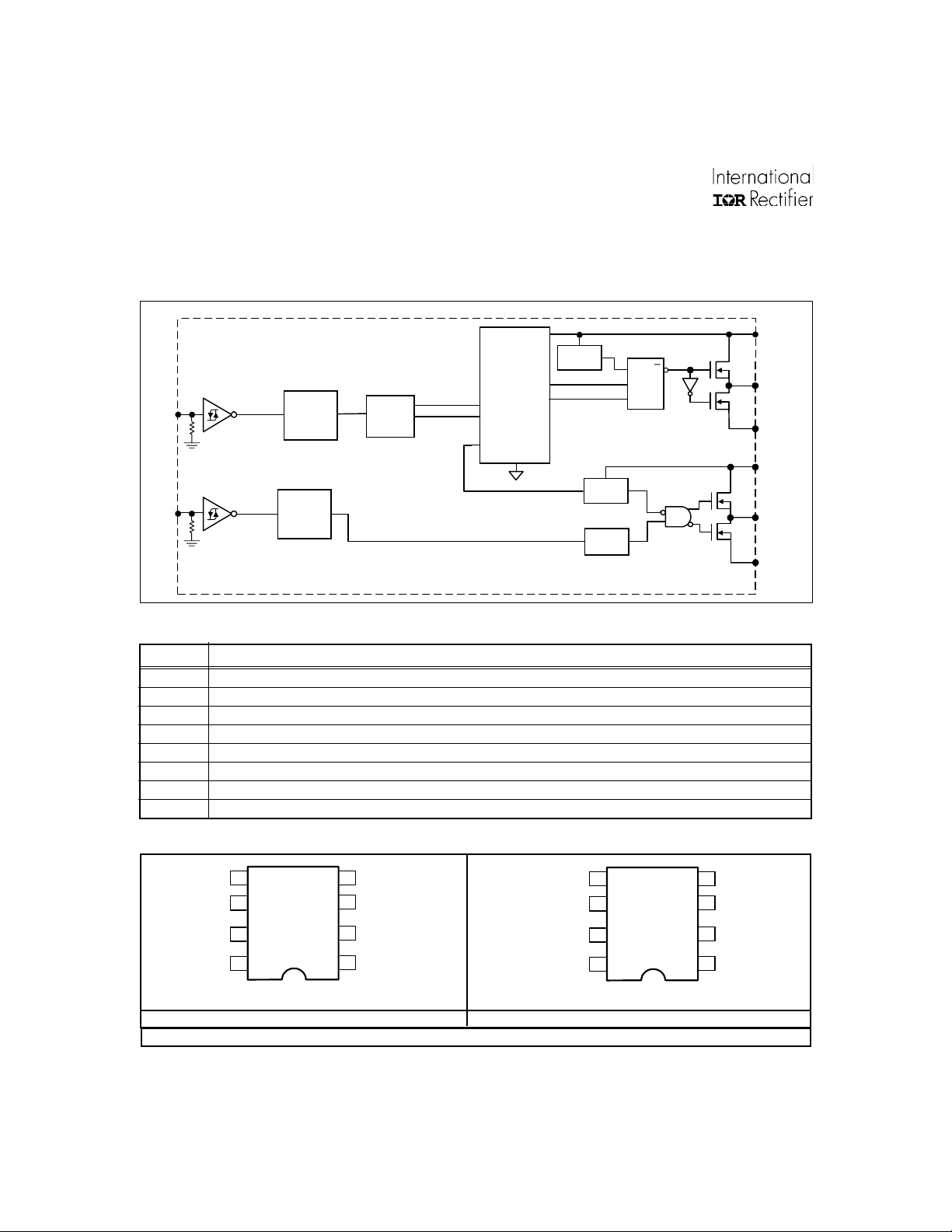
Functional Block Diagram
HIGH
VOLTAGE
3V S-TRIGGER
HIN
3V S-TRIGGER
LIN
LOW
VOLTAGE
LEVEL
SHIFT
LOW
VOLTAGE
LEVEL
SHIFT
BUFFER
Lead Definitions
Symbol Description
HIN Logic input for high side gate driver output (HO), in phase
LIN Logic input for low side gate driver output (LO), in phase
V
B
HO High side gate drive output
V
S
V
CC
LO Low side gate drive output
COM Low side return
High side floating supply
High side floating supply return
Low side supply
LEVEL
SHIFT
CIRCUIT
UV
DETECT
DETECT
UV
DELAY
UV Q
S
R
V
B
HO
V
S
V
CC
LO
COM
Lead Assignments
V
V
HO
V
CC
4
S
3
2
B
1
HIN
5
LIN
6
COM
7
LO
8
5
6
7
8
HIN
LIN
COM
LO
8-Lead PDIP 8-Lead SOIC also available LEAD-FREE (PbF)
IR2011 IR2011S
Part Number
4 www.irf.com
V
V
HO
V
CC
4
S
3
2
B
1
IR2011(S) & (PbF)
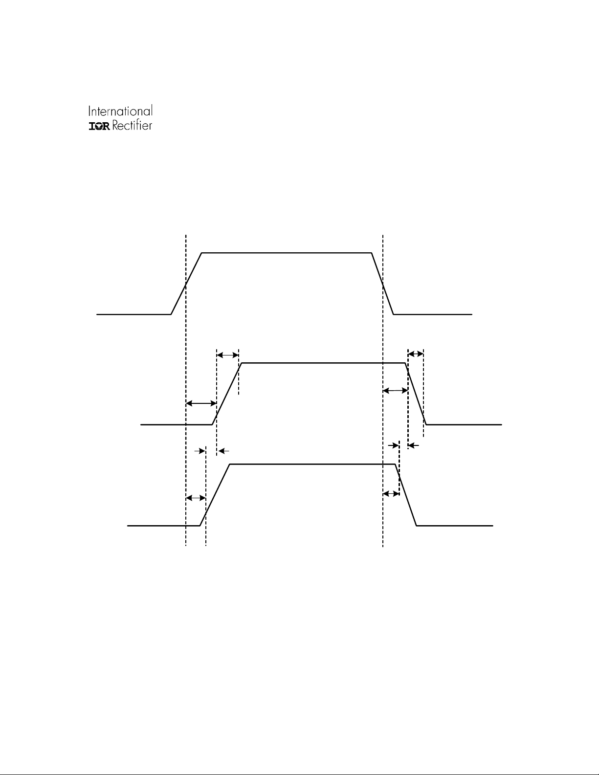
50%
ton(L)
ton(H)
10%
10%
t
rise
DM1
90%
50%
HIN / LIN
t
fall
90%
t
(H)
off
(L)
t
off
10%
DM2
90%
HO
LO
Figure 1. Timing Diagram
www.irf.com 5
IR2011(S) & (PbF)
500
400
300
200
100
Typ.
0
Turn-on Propagation Delay (ns)
-50 -25 0 25 50 75 100 125
o
Temperature (
C)
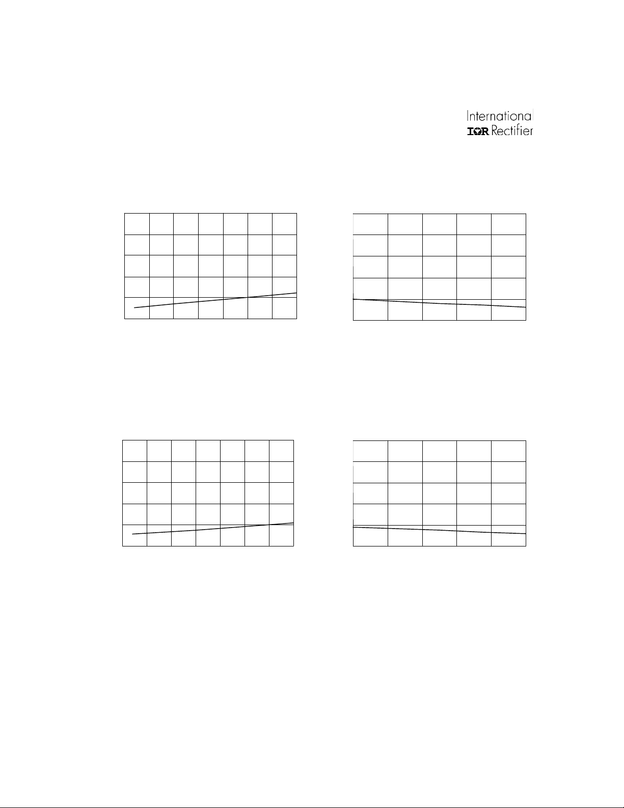
Figure 2A. Turn-on Propagation D elay
vs. Temperature
500
400
300
200
100
Typ.
500
400
300
200
Typ.
100
Turn-on Propagation Delay (ns)
0
10 12 14 16 18 20
Supply Voltage (V)
Figure 2B. Turn-on Propagation Delay
vs. Supply Voltage
500
400
300
200
Typ.
100
0
Turn-off Propagation Delay (ns)
-50 -25 0 25 50 75 100 125
o
Temperature (
C)
Figure 3A. Turn-off Propagation Delay
vs. Temperature
0
Turn-off Propagation Delay (ns)
10 12 14 16 18 20
Supply Voltage (V)
F igure 3B. Turn-off Propaga ti o n Delay
vs. Supply Voltage
6 www.irf.com

IR2011(S) & (PbF)
100
80
60
M ax.
40
Typ.
20
Turn-o n Rise Time (n s)
0
-50 -25 0 25 50 75 100 125
o
Temperature (
C)
F i gure 4A. Turn-on Rise Time vs. Temperature
50
40
M ax.
30
Typ.
20
100
80
M ax.
60
Typ.
40
20
Turn -on R ise Ti me (n s)
0
10 12 14 16 18 20
Supply Voltage (V)
F i gu re 4B. Turn-on Rise Time vs. Supply Voltage
50
M ax.
40
30
Typ.
20
10
Turn-off Fall Time (ns)
0
-50 -25 0 25 50 75 100 125
Temperature (
o
C)
Figure 5A. Turn-off Fall Time vs. Temperature
10
Turn-off Fall Time (ns)
0
10 12 14 16 18 20
Supply Voltage (V)
Figure 5B. Turn-off F all Time vs. Supply Voltage
www.irf.com 7

IR2011(S) & (PbF)
50
40
30
M ax.
20
10
Typ.
Delay Matching Time (ns)
0
-50-250 255075100125
o
Temperature (
C)
F i gure 6A. Turn-on Delay Matc hi n g Ti me
vs. Temperature
50
40
30
M ax.
20
50
40
30
M ax.
20
10
Dealy Matching Time (ns)
Typ.
0
10 12 14 16 18 20
Supply Voltage (V)
Fi gure 6B. Turn-on Delay Matching Time
vs. Supply Voltage
50
40
30
M ax.
20
10
Typ.
Delay Matching Time (ns)
0
-50 -25 0 25 50 75 100 125
o
Temperature (
C)
F i gure 7A. Turn-off Delay Matchi ng Time
vs. Temperature
10
Typ.
Dealy Matching Time (ns)
0
10 12 14 16 18 20
Supply Voltage (V)
Figure 7B. Turn-off Delay Match ing Time
vs. Supply Voltage
8 www.irf.com

IR2011(S) & (PbF)
5
4
3
Min.
2
1
Logic "1" Input Voltage (V)
0
-50 -25 0 25 50 75 100 125
o
Temperature (
C)
F i gure 8A. Logi c "1" Input Voltage
vs. Temperature
5
4
3
2
M ax.
1
Logic "0" Input Voltage (V)
0
-50-25 0 25 50 75100125
Temperature (
o
C)
5
4
3
Min.
2
1
Logic "1" Input Voltage (V)
0
10 12 14 16 18 20
Supply Voltage (V)
F i gure 8B. Logic "1" Input Voltage
vs. Supply Voltage
5
4
3
2
M ax.
1
Logic "0" Input Voltage (V)
0
10 12 14 16 18 20
Supply Voltage (V)
Fi gure 9A. Logic "0" Input Voltage
vs. Temperature
F i gu re 9B. Logi c "0" Inp ut Volta g e
vs. Supply Voltage
www.irf.com 9

IR2011(S) & (PbF)
5
4
3
M ax.
2
1
High Level Output (V)
0
-50 -25 0 25 50 75 100 125
Temperature (
o
C)
F igu re 10A. Hi gh Level O u tput vs.Temperature
0.5
0.4
0.3
0.2
M ax.
0.1
Low Level Output (V)
0.0
-50 -25 0 25 50 75 100 125
Temperature (
o
C)
5
4
3
M ax.
2
1
High Level Output (V)
0
10 12 14 16 18 20
Supply Voltage (V)
F igure 10B . High Level Output vs. Supply Volta ge
0.5
0.4
0.3
0.2
M ax.
0.1
Low Level Output (V)
0.0
10 12 14 16 18 20
Supply Voltage (V)
F i gure 11A . Lo w Level Output vs. Temperature
Figure 11B. Low Level O utput vs. Supply Voltage
10 www.irf.com

IR2011(S) & (PbF)
500
A)
µ
400
300
200
100
M ax.
0
-50 -25 0 25 50 75 100 125
Offset Supply Leakage Current (
Temperature (
o
C)
Figure 12A. Offset Supply Leakage Current
vs. Temperature
600
A)
500
µ
400
300
200
Supply Current (
100
BS
V
M ax.
0
Typ.
-50 -25 0 25 50 75 100 125
Temperature (
o
C)
500
A)
µ
400
300
200
100
0
M ax.
50 80 110 140 170 200
Offset Supply Leakage Current (
V
Boost Voltage (V)
B
600
A)
500
µ
400
300
200
Supply Current (
BS
100
V
M ax.
0
Typ.
10 12 14 16 18 20
V
Floating S u ppl y Voltage (V)
BS
www.irf.com 11

IR2011(S) & (PbF)
600
A)
500
µ
400
300
200
Supply Current (
100
CC
V
M ax.
Typ.
0
-50-25 0 25 50 75100125
Temperature (
o
C)
Figure 14A. VCC Supply Current
vs. Tempera ture
100
A)
µ
80
60
40
600
A)
500
µ
400
300
M ax.
200
Supply Current (
CC
100
V
Typ.
0
10 12 14 16 18 20
Supply Voltage (V)
V
CC
Figure 14B. VCC Supply Current
vs. V
Supply Voltage
CC
100
A)
µ
80
60
40
20
M ax.
Typ.
0
Logic "1" Input Bias Current (
-50-250 255075100125
Temperature (
o
C)
20
M ax.
0
Logic "1" Input Bias Current (
Typ.
10 12 14 16 18 20
Supply Voltage (V)
Figure 15A. L ogic "1" Input Bias Current
vs. Temperature
12 www.irf.com

IR2011(S) & (PbF)
5
A)
µ
4
3
2
M ax.
1
0
Logic "0" Input Bias Current (
-50-250 255075100125
Temperature (
o
C)
Figure 16A. Logic "0" Input Bias Current
vs. Temperature
12
11
10
M ax.
Typ.
9
UV T hreshold (+) (V)
BS
Min.
8
and V
7
CC
V
-50 -25 0 25 50 75 100 125
o
Temperature (
C)
5
A)
µ
4
3
2
M ax.
1
0
Logic "0" Input Bias Current (
10 12 14 16 18 20
Suppl y Voltage (V)
Figure 16B. Logi c "0" Input Bias Current
vs. Supply Voltage
12
11
10
M ax.
9
UV T hreshold (-) (V)
Typ.
BS
8
Min.
and V
7
CC
V
-50 -25 0 25 50 75 100 125
o
Temperature (
C)
Figure 17. VCC and VBS Undervoltage Threshold (+)
vs. Temperature
Figure 18. VCC and VBS Undervoltage Threshold (-)
vs. Temperature
www.irf.com 13

IR2011(S) & (PbF)
5
4
3
2
Typ.
1
Output Source Current (A)
0
-50 -25 0 25 50 75 100 125
o
Temperature (
C)
Figure19A. Output Source Current
vs. Temperature
5
4
3
5
4
3
2
Typ.
1
Output Source Current (A)
0
10 12 14 16 18 20
Supply Voltage (V)
F i gure 19B. Output So urce Current
vs. Supply Voltage
5
4
3
2
Typ.
1
Output Sink Current (A)
0
-50 -25 0 25 50 75 100 125
Temperature (
o
C)
Fi gure 20A. Output Sink Current
vs. Temperature
2
1
Typ.
Output Sink Current (A)
0
10 12 14 16 18 20
Supply Voltage (V)
F igure 20B. Output Sink Current
vs. Supply Voltage
14 www.irf.com

0
-3
Typ.
-6
-9
Negative Offset (V)
S
-12
-15
Maximum V
10 12 14 16 18 20
V
Floating Supply Voltage (V)
BS
Figure 21. Maximum VS Negativ e O ffset
vs. V
F l oating Su pp ly Voltage
BS
IR2011(S) & (PbF)
www.irf.com 15

IR2011(S) & (PbF)
Case outlines
A
E
D B
5
87
6
6X
0.25 [ . 010 ]
65
H
4312
0.25 [ . 010 ] A
e
8X b
e1
A1
A
CAB
NOTES:
1. DIMENSI ONING & TOLERANCING PER ASME Y14.5M-1994.
2. CONT ROLLING DIMENSION: MI L LIMETER
3. D IMENSIONS ARE SHOW N IN MILL IMETERS [INCHES].
4. OUTLINE CONFORMS TO JEDE C OUT L INE MS-01 2 A A .
C
0.10 [ . 004 ]
8-Lead PDIP
6.46 [. 2 55]
3X 1.27 [. 05 0]
y
8-Lead SOIC
01-3003 01
DIM
FOOTPRINT
8X 0.72 [. 02 8]
8X 1.78 [. 07 0]
MIN MAX
.0532
A
A1
b
c .0075 .0098 0.19 0.25
D
E
e
e1
H
K
L
y
.0688
.0040
.0098
.020
.013
.1968
.189
.1574
.1497
.050 BASI C
.025 BASIC 0.635 BASIC
.2284
.2440
.0099
.0196
.016
.050
8°
0°
K x 4 5°
8X L
8X c
7
5 DIMENSION DOES NOT INCLUDE MOLD PROTRUSIONS.
MOLD PROTRUSI ONS NOT TO EXC EED 0.15 [.006].
6 DIMENSION DOES NOT INCLUDE MOLD PROTRUSIONS.
MOLD PROTRUSI ONS NOT TO EXC EED 0.25 [.010].
7 DIMENSION IS THE L ENGT H OF L EAD FOR SOLD ERING T O
A SUBSTRATE.
01-0021 11
01-6014
(MS-001AB)
MILLIMETERSINCHES
MIN MAX
1.35
1.75
0.10
0.25
0.33
0.51
4.80
5.00
3.80
4.00
1.27 BASI C
5.80
6.20
0.25
0.50
0.40
1.27
0°
8°
01-6027
(MS-012AA)
16 www.irf.com

IR2011(S) & (PbF)
LEADFREE PART MARKING INFORMATION
Part number
Date code
Pin 1
Identifier
?
MARKING CODE
Lead Free Released
P
Non-Lead Free
Released
IRxxxxxx
YWW?
ORDER INFORMATION
Basic Part (Non-Lead Free)
8-Lead PDIP IR201 1 order IR2011
8-Lead SOIC IR201 1S order IR2011S
IR logo
?XXXX
Lot Code
(Prod mode - 4 digit SPN code)
Assembly site code
Per SCOP 200-002
Leadfree Part
8-Lead PDIP IR2011 Not available
8-Lead SOIC IR2011S order IR2011SPbF
This product has been designed and qualified for the industrial market.
Qualification Standards can be found on IR’s Web Site http://www.irf.com/.
WORLD HEADQUARTERS: 233 Kansas Street, El Segundo, California 90245 Tel: (310) 252-7105
www.irf.com 17
Data and specifications subject to change without notice
5/25/2004
 Loading...