International Rrectifier IR1150-S -PbF User Manual
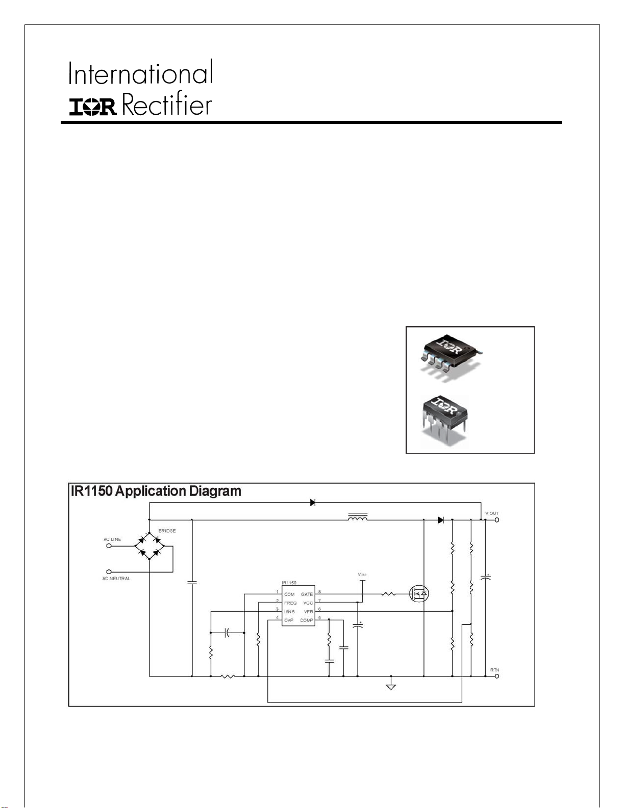
µPFC ONE CYCLE CONTROL PFC IC
Features
• PFC with IR proprietary “One Cycle Control”
• Continuous conduction mode (CCM) boost type PFC
• No line voltage sense required
• Programmable switching frequency (50kHz-200kHz)
• Programmable output overvoltage protection
• Brownout and output undervoltage protection
• Cycle-by-cycle peak current limit
• Soft start
• User initiated micropower “Sleep Mode”
Description
The µPFC IR1150 is a power factor correction (PFC) control IC designed to
operate in continuous conduction mode (CCM) over a wide range input line
voltages. The IR1150 is based on IR's proprietary "One Cycle Control" (OCC)
technique providing a cost effective solution for PFC.
The proprietary control method allows major reductions in component count,
PCB area and design time while delivering the same high system performance
as traditional solutions.
The IC is fully protected and eliminates the often noise sensitive line voltage
sensing requirements of existing solutions.
The IR1150 features include programmable switching frequency,
programmable dedicated over voltage protection, soft start, cycle- by-cycle
peak current limit, brownout, open loop, UVLO and micropower startup current.
In addition, for low standby power requirements (Energy Star, 1W
Standby, Blue Angel, etc.), the IC can be driven into sleep mode with total
current consumption below 200µA, by pulling the OVP pin below 0.62V.
Data Sheet No. PD60230 revD
IR1150(S)(PbF)
IR1150I(S)(PbF)
• Open loop protection
• Maximum duty cycle limit of 98%
• User programmable fixed frequency operation
• Min. off time of 150-350ns over freq range
• VCC under voltage lockout
• Internally clamped 13V gate drive
• Fast 1.5A peak gate drive
• Micropower startup (<200 µA)
• Latch immunity and ESD protection
• Parts also available Lead-Free
Packages
8-Lead SOIC
8-Lead PDIP
www.irf.com 1
IR1150(S)/IR1150I(S)(PbF)
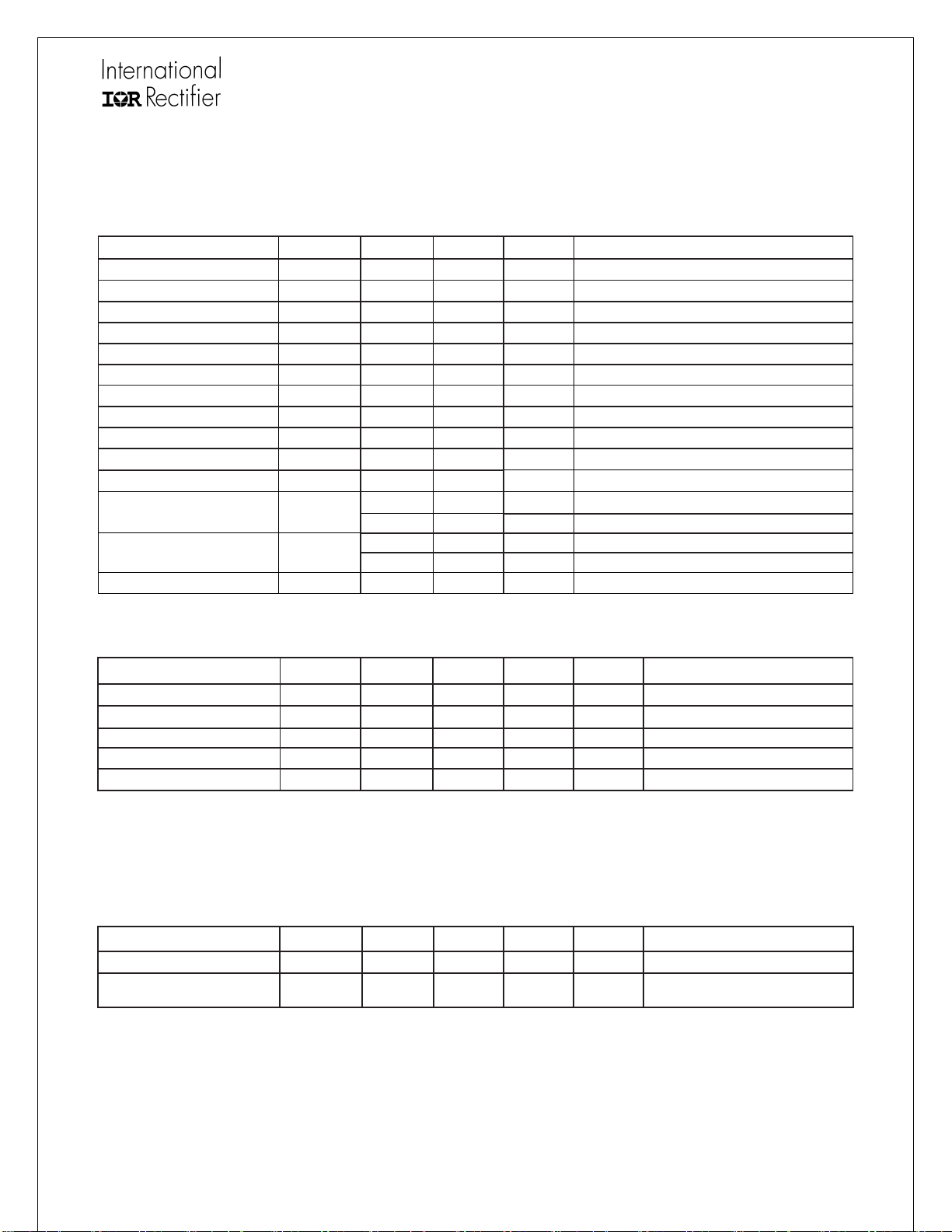
Absolute Maximum Ratings
Absolute maximum ratings indicate sustained limits beyond which damage to the device may occur. All voltages are
absolute voltages referenced to COM. Thermal resistance and power dissipation are measured under board mounted and
still air conditions.
Parameters Symbols Min. Max.
V
VCC voltage
Freq. voltage
ISNS voltage
OVP/EN voltage
VFB voltage
COMP voltage
Gate voltage
Continuous gate current
Max peak gate current
Junction temperature
Storage temperature
Thermal resistance R
Package power dissipation PD
ESD protection
CC
V
FREQ
V
ISNS
V
OVP/EN
VFB -0.3 10.5 V
V
COMP
V
GATE
I
GATE
I
GATEPK
T
T
θ JA
V
ESD
Units
Remarks
-0.3 22 V
. -0.3 10.5 V
-10 3 V
-0.3 9 V
-0.3 10 V
-0.3 18 V
-5 5 mA
-1.5 1.5 A
-40 150 ˚C
J
-55 150 ˚C
S
— 2 kV
— 128 ˚C/W
— 84 ˚C/W
— 675 mW
— 1000 mW
Not internally clamped
SOIC-8
PDIP-8
SOIC-8 T
PDIP-8 T
AMB
= 25 ˚C
AMB
= 25 ˚C
Human body model*
Recommended Operating Conditions
Recommended operating conditions for reliable operation with margin
Parameters Symbols Min. Typ. Max. Units Remarks
Supply voltage VCC 15 18 20 V
Junction temperature TJ -25 — 125 °C
Ambient temperature TA 0 — 70 °C IR1150(S)
Ambient temperature TA -25 — 85 °C IR1150I(S)
Switching frequency FSW 50 — 200 kHz
Electrical Characteristics
The electrical characteristics involve the spread of values guaranteed within the specified supply voltage and junction
temperature range T
not otherwise stated, a supply voltage of V
Supply Section
Parameters Symbols
VCC turn-on threshold VCC ON 12.2 12.7 13.2 V
VCC turn-off threshold
(under voltage lock out)
*Per EIA/JESD22-A114-B (discharging a 100pF capacitor through a 1.5KΩ series resistor)
from – 25°C to 125°C. Typical values represent the median values, which are related to 25°C. If
J
VCC UVLO 10.2 10.7 11.2 V
=15V is assumed for test condition
CC
Min.
Typ. Max.
Units
Remarks
www.irf.com
2
IR1150(S)/IR1150I(S)(PbF)
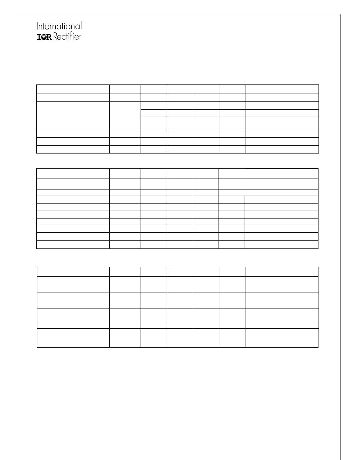
Electrical Characteristics cont.
The electrical characteristics involve the spread of values guaranteed within the specified supply voltage and junction
temperature range T
otherwise stated, a supply voltage of V
Parameters Symbols Min. Typ. Max. Units Remarks
VCC turn-off hysteresis VCC HYST 1.8 — 2.2 V
Operating current ICC
Startup current I
Sleep current I
Sleep threshold V
Oscillator Section
Parameters Symbols Min. Typ. Max. Units Remarks
Switching frequency fSW 50 — 200 kHz R
Initial accuracy f
Voltage stability V
Temperature stability T
Total variation fVT — 10 — % Line & temperature
Long term stability F
Maximum duty cycle D
Minimum duty cycle D
Minimum off time T
Protection Section
Parameters Symbols Min. Typ. Max. Units Remarks
Open loop protection(OLP)
Vfb threshold
Output under voltage
protection (OUV)
Output over voltage
protection (OVP)
OVP hysteresis — 350 450 550 mV
Peak current limit protection
(I
) I
PKLMT
threshold
voltage
SNS
from – 25°C to 125°C. Typical values represent the median values, which are related to 25°C. If not
J
=15V is assumed for test condition.
CC
— 18 22 mA C
— 36 40 mA C
— 8 10 mA
— — 175 uA VCC=VCC ON - 0.1V
CCSTART
— 125 200 uA V
SLEEP
0.56 0.62 0.68 V
SLEEP
— — 5 % TA = 25˚C
SW ACC
— 0.2 3 % 13V <VCC <20V
STAB
— 2 — % -25˚C ≤ TJ≤ 125˚C
STAB
— 0.1 0.5 % T
STABLT
93 — 98 % fSW=200kHz
MAX
— — 0 %
MIN
200 300 400 Ns fSW= 50kHz to 200kHz
offmin
=1nF fSW=200kHZ
LOAD
=10nF fSW=200kHZ
LOAD
Standby mode - inactive gate
Internal oscillator running
<0.5V, VCC =15V
OVP
= 165kΩ-37kΩ approx.
SET
= 125˚C, 1000Hrs
AMB
V
17 19 21 %VREF
OLP
V
49 51 53 %VREF Brown out protection
OUV
V
104 105.5 107 %VREF
OVP
V
-1.11 -1.04 -0.96 V
ISNS
www.irf.com
3
IR1150(S)/IR1150I(S)(PbF)
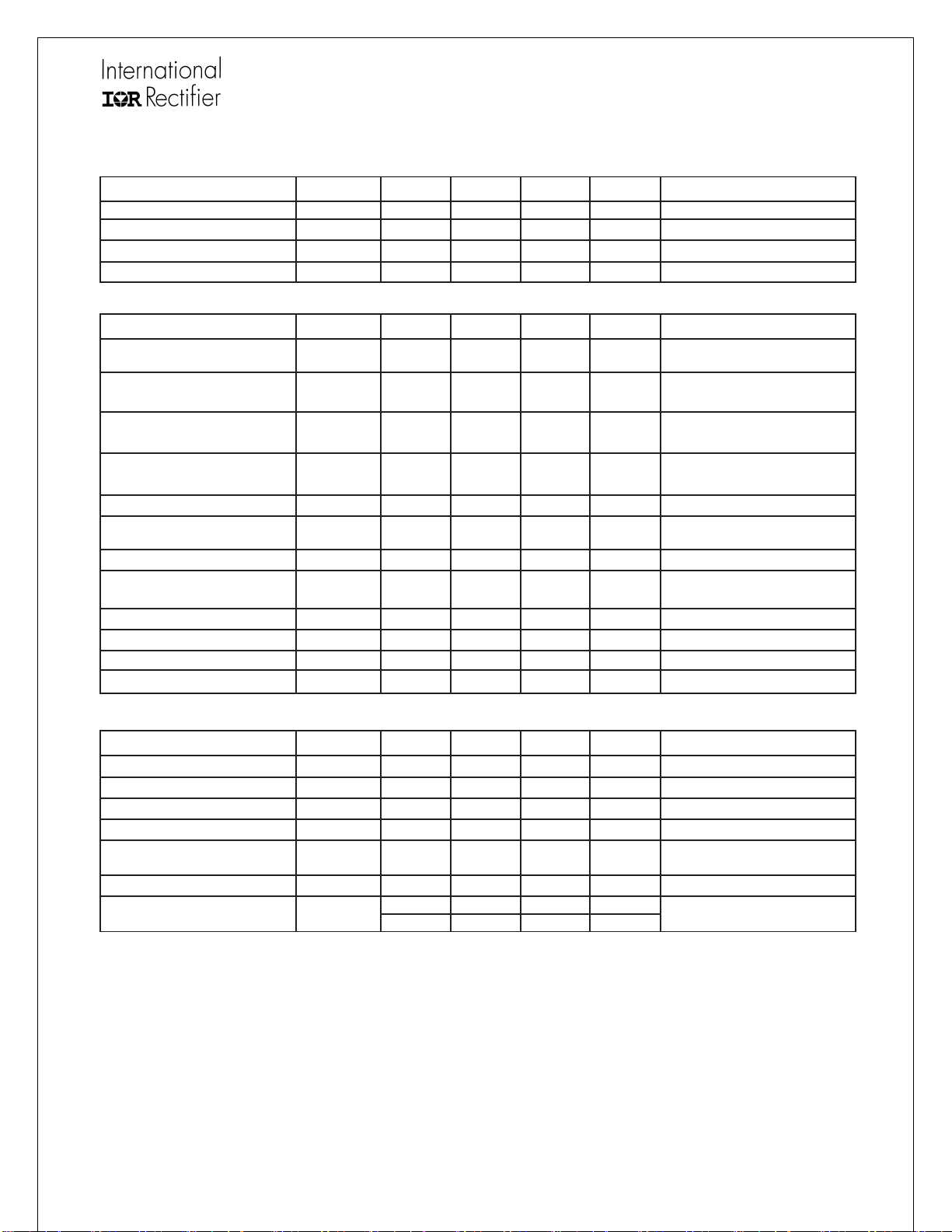
Internal Voltage Reference Section
Parameters Symbols Min.
Reference voltage V
Line regulation R
Temp stability T
Total variation ∆V
Voltage Error Amplifier Section
6.9 7.0 7.1 V TA = 25˚C
REF
— 12 25 mV 13.5V <VCC < 20V
REG
— 0.4 — % -25˚C ≤T
STAB
6.8 — 7.1 V Over VCC and Tj ranges
TOT
Parameters Symbols Min.
Typ.
Typ.
Max.
Max.
Units
Remarks
Units
Remarks
Transconductance gm 30 40 55 µS -25˚C ≤T
Source/sink current
Soft start delay time
(calculated)
VCOMP voltage (fault) V
Effective VCOMP voltage V
I
OVEA
t
— 40 — ms
ss
COMP FLT
COMP EFF
Input bias current IIB — -0.2 -0.5 µA
Open loop bandwidth BW — 1 — MHz
Input offset voltage temp
coefficient
Common mode rejection ratio
TC
— — 10 µV/˚C Note 1
IOV
CMRR — 100 — dB
Output low voltage VOL — — 0.5 V
Output high voltage VOH 5.71 6.15 6.8 V
VCOMP start voltage V
COMP START
30
20
— 1.2 1.5
0.2
40
45
65
90
µA
V
T
-25˚C ≤T
6.05 V
300 500 700 mV
AMB
R
GAIN
C
POLE
@ 1mA (max) initial
@ 25µA steady state
V
FB
-25˚C ≤ T
≤ 125˚C
AMB
≤ 125˚C
AMB
= 25˚C
≤ 125˚C
AMB
=1kΩ , C
ZERO
=0.33µF
=0.01µF, fXO=28Hz
=0V
≤ 125˚C
AMB
Current Amplifier Section
Parameters Symbols Min.
Typ.
Max.
Units
Remarks
DC gain gDC — 2.5 — V/V
Corner frequency fC 200 — 280 kHz Note 1
Input offset voltage VIO — 1 4 mV Note 1
ISNS bias current ΙIB — 200 300 µA VFB=0V,-25˚C ≤ T
Input offset voltage temp
coefficient
Common mode rejection ratio
Blanking time T
www.irf.com
TC
— — 10 µV/˚C Note 1
IOV
CMRR — 100 — dB
BLANK
230 350 450 ns
150 600 ns
= 25˚C
T
AMB
-25˚C ≤T
≤ 125˚C
AMB
AMB
≤ 125˚C
4
IR1150(S)/IR1150I(S)(PbF)
Gate Driver Section
Parameters Symbols Min. Typ. Max. Units Remarks
Gate low voltage V
Gate high voltage V
Gate high voltage V
Rise time tr
Fall time tf
Out peak current I
Gate voltage @ fault VG
Note 1: Guaranteed by design, but not tested in production.
— 1.2 1.5 V I
GLO
— 13 18 V VCC=20V
GTH
9.5 — — V VCC =11.5V
GTH
— 20 — ns C
— 70 — ns C
— 20 — ns C
— 70 — ns C
1.5 — — A C
OPK
— — 1.8 V I
fault
GATE
LOAD
LOAD
LOAD
LOAD
LOAD
GATE
=200mA
= 1nF, VCC=16V
= 10nF, VCC=16V
= 1nF, VCC=16V
= 10nF, VCC=16V
= 10nF, VCC=16V
=20mA
www.irf.com
5
 Loading...