International Rrectifier IPS7081-R -S PbF User Manual
INTELLIGENT POWER HIGH SIDE SWITCH
Features
• Over temperature shutdown (with auto-restart)
• Short circuit protection (current limit)
• Active clamp
• Open load detection
• Logic ground isolated
• ESD protection
• Ground loss prot
• Status feedback
escription
D
The IPS7081(R)(S
Switch (IPS) with built in short circuit, over-temperature,
ESD protection, inductive load capability and diagnostic
feedback. The output current is limited at Ilim value.
Current limitation is activated until the thermal protection
acts. The over-temperature protection turns off the device
if the junction temperature exceeds Tshutdown. It will
automatically restart after the junction has cooled 7°C
below Tshutdown. A diagnostic pin is provided for status
feedback of short circuit, over-temperature and open load
detection. The double level shifter circuitry allows large
offsets between the logic ground and the load.
)PbF is a five terminal Intelligent Power
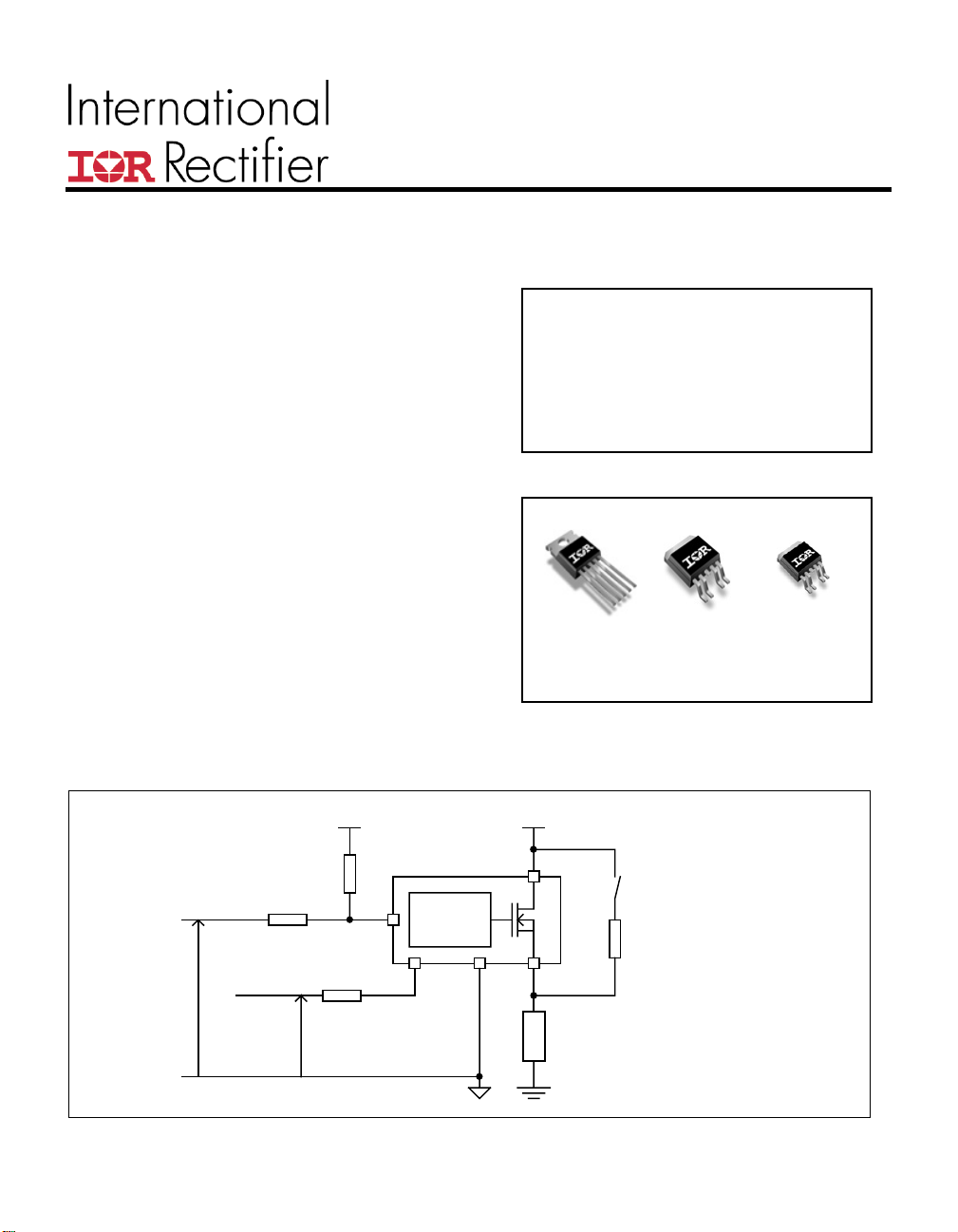
Typical Connection
from power ground
ection
+5V
Data sheet N° PD60308
IPS7081(R)(S)PbF
Product Summary
Rds(on) 70mΩ max.
Vclamp 70V
I Limit 5A (typ.)
Open load 3V
Package
TO220 D²Pak D-Pak
IPS7081PbF IPS7081SPbF IPS7081RPbF
+Bat
V Diag
www.irf.com
Rdg Pull-up resistor for Open
Input Signal
15K
Dg(4)
In(2) Gnd(1)
Rin
Vcc(3)
Control
Load Off detection
Out(5)
Load
1
IPS7081(R)(S)
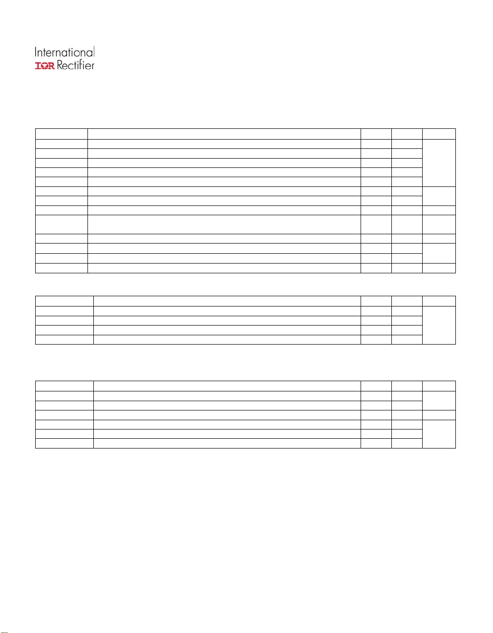
Absolute Maximum Ratings
Absolute maximum ratings indicate sustained limits beyond which damage to the device may occur. All voltage parameters
are referenced to Ground lead. (Tambient=25°C unless otherwise specified).
Symbol Parameter Min. Max. Units
Vout Maximum output voltage Vcc-65 Vcc+0.3
Voffset Maximum logic ground to load ground offset Vcc-65 Vcc+0.3
Vin Maximum input voltage -0.3 5.5
Vcc max. Maximum Vcc voltage
Vcc cont. Maximum continuous Vcc voltage
Iin max. Maximum IN current -1 10
Idg max. Maximum diagnostic output current -1 10
Vdg Maximum diagnostic output voltage -0.3 5.5 V
Pd
Isd cont. Maximum continuous diode current (Rth=50°C/W)
ESD1
ESD2
Tj max. Max. storage & operating temperature junction temperature -40 +150 °C
Maximum power dissipation (internally limited by thermal protection)
Rth=50°C/W
Electrostatic discharge voltage (Human body) 100pF, 1500Ω
Electrostatic discharge voltage (Machine Model) C=200pF,R=0Ω,L=10µH
⎯
⎯
⎯
⎯
⎯
⎯
65
35
2.5 W
2.2 A
4
0.5
Thermal Characteristics
Symbol Parameter Typ. Max. Units
Rth1 Thermal resistance junction to ambient D-Pak std. footprint 70
Rth2 Thermal resistance junction to ambient D-Pak 1” sqrt. footprint 50
Rth3 Thermal resistance junction to case D-Pak / TO220 / D²Pak 3
Rth1 Thermal resistance junction to ambient TO220 free air 60
⎯
⎯
⎯
⎯
Recommended Operating Conditions
These values are given for a quick design. For operation outside these conditions, please consult the application notes.
Symbol Parameter Min. Max. Units
VIH High level input voltage 4 5.5
VIL Low level input voltage -0.3 0.9
Iout Continuous drain current, Tamb=85°C, Tj=125°C, Vin=5V, Rth=50°C/W
Rin Recommended resistor in series with IN pin 4 10
Rdgs Recommended resistor in series with DG pin 10 20
Rol Recommended pull-up resistor for open load detection 5 100
⎯
2.3 A
V
mA
kV
°C/W
kΩ
www.irf.com
2
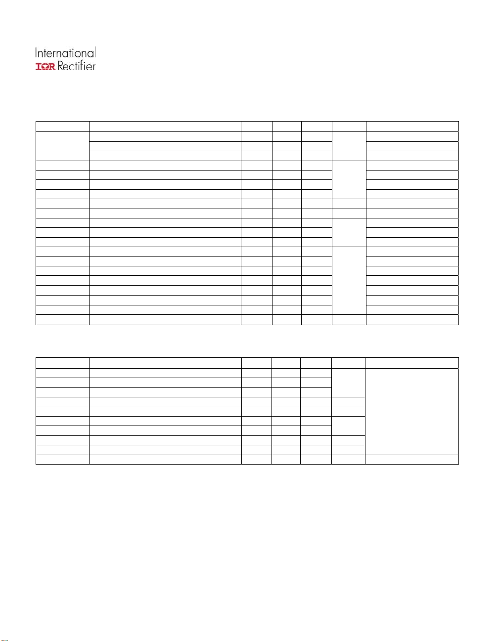
Static Electrical Characteristics
Tj=25°C, Vcc=14V (unless otherwise specified)
Symbol Parameter Min. Typ.
Rds(on)
ON state resistance Tj=150°C
ON state resistance Tj=25°C, Vcc=6.5V Vin=5V, Iout=2A
ON state resistance Tj=25°C
Vcc op. 6
Operating voltage range
V clamp 1 Vcc to Out clamp voltage 1 65 70
V clamp 2 Vcc to Out clamp voltage 2
Vf Body diode forward voltage
Icc Off Supply current when Off
Icc On
Supply current when On
Iout@0V V 0V Output leakage current
Iout@6V utput leakage current 20
Idg leakage
O
Diagnostic output leakage current
Vdgl Low level diagnostic output voltage
Vih Input high threshold voltage
Vil Input low threshold voltage
In hys Input hysteresis 0.15 0.5 1
UV high Under voltage high threshold voltage
UV low Under voltage low threshold voltage 3.4 4.5
UV hys U 1.5
ndervoltage hysteresis 0.1 0.5
Iin On In µA V V put current when device is On
S hing E
witc lectrical Characteristics
cc=14V, Resistive load=6Ω, Vin=5V, Tj=25°C
V
Symbol Parameter M
Tdon Turn-on delay time
Tr1 Rise time to Vout=Vcc-5V
Tr2
dV/dt (On) T
EOn T
Tdoff Turn-off delay time
Tf F
dV/dt (Off) T
EOff T
Tdiag Vout to Vdiag propagation delay
Rise time to Vout=0.9 x Vcc
urn On dV/dt
urn On energy
all time to Vout=0.1 x Vcc
urn Off dV/dt
urn Off energy
⎯
⎯
⎯
⎯
⎯
⎯
⎯
⎯
⎯
⎯
⎯
⎯
1
⎯
⎯
in. Typ. Max. Units Test Conditions
⎯
⎯
⎯
⎯
⎯
⎯
⎯
⎯
⎯
⎯
Max. Units Test Conditions
55 70 , Vin=5V Iout=2A
100 130 Vin=5V, Iout=2A
60 80
⎯
35
70 75 Iout=2A (see Fig. 1)
1 1.35
2.5 10 µA V V, Vout=0V in=0
2.5 3.5 mA V
2.5 10 out=
⎯
10
0.2 0.3 Idg=1.6mA
2.5 3.5
2
5 5.9
40 80 in=5
16 45
10 40
20 100
0.8 3 V/µs
100
⎯
25 50
7.5 25
1.6 3 V/µs
25
15
⎯
⎯
⎯
⎯
⎯
⎯
mΩ
V
µA
V
µs
µJ
µs
µJ
µs See Fig. 4 and Fig. 12
IPS7081(R)(S)
Iout=30mA (see Fig. 1)
Io 2.5Aut=
Vin=5
Vout=6V
V 5.5V
dg=
S g. 3
ee Fi
www.irf.com
3
IPS7081(R)(S)
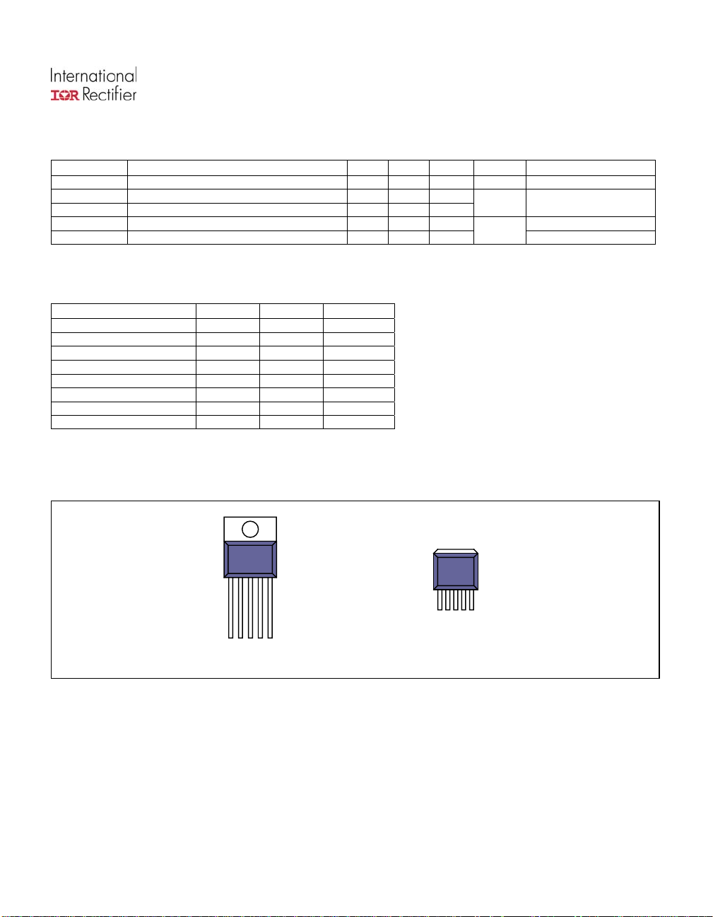
Protection Characteristics
Symbol Parameter Min. Typ. Max. Units Test Conditions
Ilim Internal current limit 2 7 10 A Vout=0V
Tsd+ Over temperature high threshold 150
Tsd- Over temperature low threshold
Vsc Short-circuit detection voltage
Vopen load Open load detection threshold
(1
)
Guarantee y design
(2
)
Reference Vcc
d b
to
(2)
T Tabl
ruth e
Operatin onditions IN
g C OUT DG pin
Normal H H H
Normal L L L
Open Load H H H
Open Load
(3)
Short circuit to imiting) L Gnd H L (l
Short circuit to L Gnd L L
Over-temperature H L (cycling) L
Over-temperature L L L
(3
)
With a p resistor connected between the outpu cc.
ull-up t and V
Lead Assignments
3- Vcc
1 2 3 4 5
TO220
⎯
2
2
HL H
1- Gn
d
2- In
3- Vc
c
4- Dg
5- Ou
t
(1)
165
158
⎯
⎯
°C See Fig. 2
3 4
3 4
c
3- Vc
1 2 3 4 5
a D²Pa
D-P k - k
V
www.irf.com
4
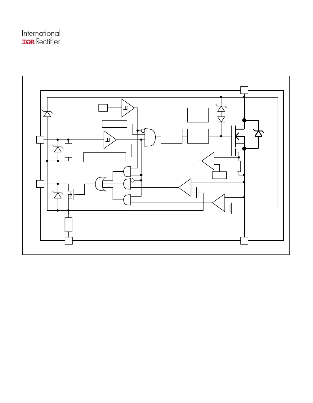
Functional Block Diagram
V
All values are typical
165°C
Tj
158°C
Vcc-Gnd >UV
2.5V
2.0V
IN
DG
6V
6V
75V
150kΩ
Gnd Protection Loss
LevelSh
ifter
Open Load
Short Circuit
Charge
+
Pump
Driver
3V
IPS7081(R)(S)
CC
66V
-
+
I Sense
I Limit
-
+
3V
75V
30Ω
GND
OUT
www.irf.com
5
 Loading...