

Page 1

IRDC3863
SupIRBuck
TM
USER GUIDE FOR IRDC3863 EVALUATION BOARD
DESCRIPTION
TM
The IR3863 SupIRBuck
fully integrated and highly efficient DC/DC
voltage regulator. The onboard constant on
time hysteretic controller and MOSFETs make
IR3863 a space-efficient solution that delivers
up to 6A of precisely controlled output voltage
in a 4mm x 5mm QFN package.
In addition to excellent light load and full load
efficiency, the IR3863 offers features such as:
a 0.5V reference, programmable switching
frequency, temperature compensated over
current protection, thermal shutdown and
optional forced continuous conduction mode.
is an easy-to-use,
Additional features include: pre-bias startup,
soft start, power good output, enable input with
voltage monitoring capability and over/under
voltage protection, making the device a very
flexible solution that is suitable for a broad
range of applications.
This user guide contains the schematic, bill of
materials, and operating instructions of the
IRDC3863 evaluation board. Detailed product
specifications, application information and
performance curves at different operating
conditions are available in the IR3863 data
sheet.
BOARD FEATURES
• V
= +12V
IN
• V
• V
• I
• F
= +5V
CC
= +1.05V
OUT
= 0 to 6A
OUT
= 300kHz @ CCM
S
• L = 2.2µH
• C
• C
= 22µF
IN
= 47µF (ceramic 0805) + 150µF (PC-CON)
OUT
(ceramic 1210) + 68µF (electrolytic)
1
Page 2
IRDC3863
CONNECTIONS and OPERATING INSTRUCTIONS
An input supply in the range of 7 to 16V should be connected from VIN to PGND. A maximum load
of 6A may be connected to V
and PGND. The connection diagram is shown in Fig. 1,
OUT
inputs and outputs of the board are listed in Table 1.
IRDC3863 has two input supplies, one for biasing (VCC) and the other for input voltage (VIN).
Separate supplies should be applied to these inputs. VCC
5.5V supply connected to VCC and PGND. Enable (EN) is controlled
input should be a well regulated 4.5V to
by the first switch of SW1, and
FCCM option can be selected by the second switch of SW1. Toggle the switch to the ON position
(marked by a solid square) to enable switching or to select FCCM. The absolute maximum voltage
of the external signal applied to EN (TP4) and FCCM is +8V.
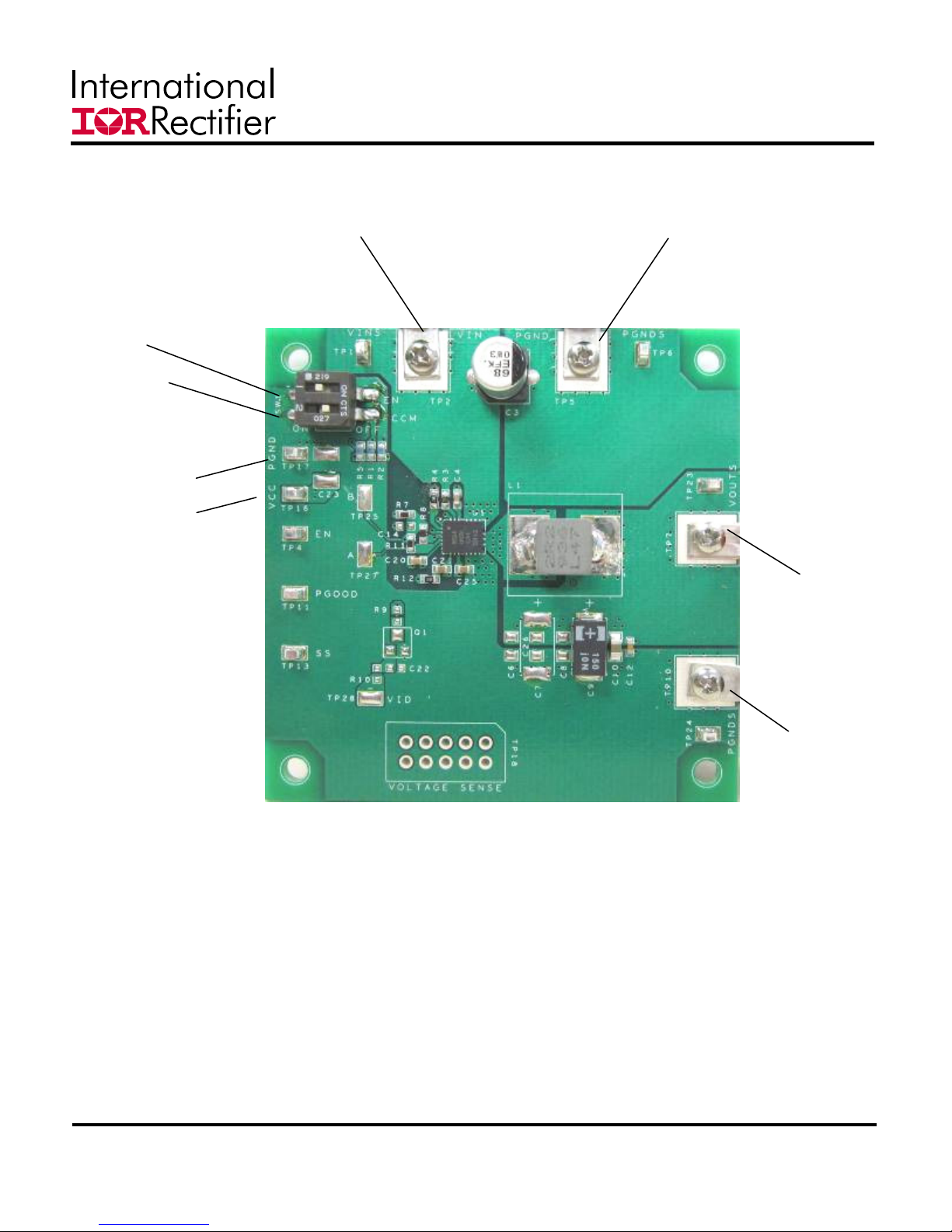
Table 1. Connections
Connection Signal Name
VIN (TP2) VIN
PGND (TP5) Ground for VIN
and the
VCC (TP16) VCC Input
PGND (TP17) Ground for VCC Input
VOUT (TP7) V
PGND (TP10) Ground for V
EN (TP4) Enable Input
OUT
(+1.05V)
OUT
LAYOUT
The PCB is a 4-layer board. All layers are 1 oz. copper.
on the top and bottom layers of the board.
The power supply decoupling capacitors, bootstrap capacitor and feedback components are located
close to IR3863. To improve efficiency, the circuit board is designed to minimize the length of the onboard power ground current path.
IR3863 and other components are
mounted
2
Page 3
CONNECTION DIAGRAM
IRDC3863
Control Switch for:
EN
FCCM
GROUND
VCC = +5.0V
VIN
GROUND
VOUT = +1.05V
Fig. 1: Connection Diagram of IRDC3863 Evaluation Board
GROUND
3
Page 4
PCB Board Layout
IRDC3863
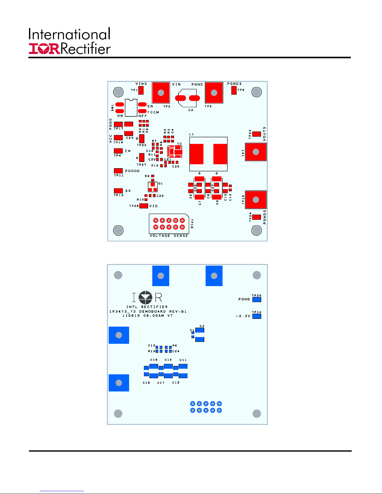
Fig. 2: Board Layout, Top Components
Fig. 3: Board Layout, Bottom Components
4
Page 5

PCB Board Layout
IRDC3863
Fig. 4: Board Layout, Top Layer
Fig. 5: Board Layout, Bottom Layer
5
Page 6

PCB Board Layout
IRDC3863
Fig. 6: Board Layout, Mid-layer I
Fig. 7: Board Layout, Mid-layer II
6
Page 7

IRDC3863
TP7
VOUT
TP23
VOUTS
VOUT
TP2
VIN
TP1
VINS
VIN
TP5
PGND
TP6
PGNDS
C3
68uF
+
C2
22uF
C1
1uF
L1
2.2uH
VSW
C4
0.22uF
U1
IR3863
13
R3
200K
14
15
16
17
TP10
PGND
TP24
PGNDS
C27
IR3863
GND14FB
5
open
C26
open
C19
open
C18
open
C17
open
C16
open
C15
open
C24
open
PGND
11
VCC
10
NC2
9
3VCBP
8
SS
NC1
6
7
C21
C12
0.1uF
C11
open
C10
47uF
C9
150uF
C8
open
C7
open
C6
open
R13
open
C13
open
R6
open
12
VIN
FF
EN
PHASE
BOOT
GND
FCCM
PGOOD
ISET
1
3
2
TP18
VOLTAGE SENSE
10
9
8
7
6
R7
2.80K
C14
open
C25
1uF
1uF
R12
4.99
+Vout2s5-Vout2s
+Vout1s
-Vout1s
-Vdd2s
-Vdd1s
-Vins
VOUT
4
+Vdd2s
+3.3V
3
+Vdd1s
VCC
2
+Vins
VIN
1
R8
2.55K
R9
open
Q1
open
2
3
1
TP25
B
20
R11
TP27
A
C22
open
R10
open
TP28
VID
Fig. 8: Schematic of the IRDC3863 Evaluation Board
ISET
FCCM
EN
R4
10K
R1
10K
+3.3V
R2
10K
VCC
EN
TP4
VSW
2
3
1
4
SW1
EN / F CCM
C20
PGOOD
R5
10K
+3.3V
TP11
PGOOD
0.1uF
FB
SS
TP13
SS
+3.3V
TP14
+3.3V
TP26
AGND
C23
open
VCC
TP17
PGND
TP16
VCC
7
Page 8

Bill of Materials
IRDC3863
8
Page 9

TYPICAL OPERATING WAVEFORMS
Tested with demoboard shown in Fig. 8, VIN = 12V, VCC = 5V, VOUT
unless otherwise specified
IRDC3863
= 1.05V, Fs = 300kHz, TA= 25oC, no airflow,
EN
PGOOD
SS
VOUT
5V/div
5V/div 1V/div 500mV/div 5ms/div 5V/div 5V/div 1V/div 500mV/div 1ms/div
Fig. 9: Startup
Fig. 10: Shutdown
VOUT
PHASE
i
L
EN
PGOOD
SS
VOUT
VOUT
PHASE
i
L
20mV/div 10V/div 500mA/div 5µs/div 20mV/div 10V/div 2A/div 2µs/div
PGOOD
Fig. 11: DCM (I
OUT
= 0.1A)
Fig. 12: CCM (I
OUT
= 5A)
PGOOD
SS
VOUT
I
OUT
5V/div 1V/div 500mV/div 2A/div 50µs/div5V/div 1V/div 1V/div 5A/div 500µs/div
Fig. 13: Over Current Protection (tested by
shorting VOUT to PGND)
Fig. 14: Over Voltage Protection
(tested by shorting FB to VOUT)
FB
VOUT
i
L
9
Page 10

TYPICAL OPERATING WAVEFORMS
Tested with demoboard shown in Fig. 8, VIN = 12V, VCC = 5V, VOUT
unless otherwise specified
IRDC3863
= 1.05V, Fs = 300kHz, TA= 25oC, no airflow,
VOUT
PHASE
i
L
10V/div
2A/div
Fig. 15: Load Transient 0-2A
50µs/div
50mV/div
10V/div 2A/div 50µs/div50mV/div
Fig. 16: Load Transient 3-5A
TYPICAL PERFORMANCE
VIN = 12V, VCC = 5V, VOUT = 1.05V, Fs = 300kHz, IOUT = 6A, TA= 25oC, no airflow
VOUT
PHASE
i
L
Fig. 17: Thermal Image (IR3863: 60oC, Inductor: 45oC, PCB: 32oC)
10
Page 11

TYPICAL OPERATING DATA
VIN = 12V, VCC = 5V, VOUT = 1.05V, Fs = 300kHz, IOUT = 0 ~ 6A, TA= 25oC, no airflow,
unless otherwise specified
IRDC3863
90%
85%
80%
75%
70%
65%
Efficiency
60%
55%
50%
45%
0.01 0.1 1 10
Load Current (A)
Fig. 18: Efficiency vs. Load Current
1.090
1.085
1.080
1.075
1.070
1.065
1.060
1.055
Output Voltage (V)
1.050
1.045
1.040
0123456
Load Current (A)
350
300
250
200
150
100
50
Switching Frequency (kHz)
0
0123456
Load Current (A)
Fig. 19: Switching Frequency vs. Load Current
1.090
1.085
1.080
1.075
1.070
1.065
1.060
1.055
Output Voltage (V)
1.050
1.045
1.040
7 8 9 10111213141516
Input Voltage (V)
Fig. 20: Load Regulation
Fig. 21: Line Regulation at 6A Load
11
Page 12

IRDC3863
PCB Metal and Components Placement
Lead lands (the 13 IC pins) width should be equal to nominal part lead width. The minimum lead to lead spacing
should be ≥ 0.2mm to minimize shorting.
Lead land length should be equal to maximum part lead length + 0.3 mm outboard extension. The outboard
extension ensures a large toe fillet that can be easily inspected.
Pad lands (the 4 big pads) length and width should be equal to maximum part pad length and width. However, the
minimum metal to metal spacing should be no less than 0.17mm for
Copper, or no less than 0.23mm for 3 oz. Copper.
2 oz. Copper, or no less than 0.1mm for 1 oz.
12
Page 13

IRDC3863
Solder Resist
It is recommended that the lead lands are Non Solder Mask Defined (NSMD). The solder resist should be pulled
away from the metal lead lands by a minimum of 0.025mm to ensure
NSMD pads.
The land pad should be Solder Mask Defined (SMD), with a minimum
0.05mm to accommodate solder resist misalignment.
Ensure that the solder resist in between the lead lands and the pad land is ≥ 0.15mm due to the high aspect ratio of
the solder resist strip separating the lead lands from the pad land.
overlap of the solder resist onto the copper of
13
Page 14

Stencil Design
IRDC3863
The Stencil apertures for the lead lands should be approximately
amount of solder deposited will minimize the occurrences of lead
center pad, the part will float and the lead lands will open.
The maximum length and width of the land pad stencil aperture should be equal to the solder resist opening minus
an annular 0.2mm pull back in order to decrease the risk of shorting the center land to the lead lands when the part
is pushed into the solder paste.
80% of the area of the lead lads. Reducing the
shorts. If too much solder is deposited on the
14
Page 15

IRDC3863
IR WORLD HEADQUARTERS:
233 Kansas St., El Segundo, California 90245, USA Tel: (310) 252-7105
TAC Fax: (310) 252-7903
Visit us at www.irf.com for sales contact information
Data and specifications subject to change without notice. 06/2011
15
 Loading...