International Rectifier ST380C06C3L, ST380C06C3, ST380C06C2L, ST380C04C0L, ST380C06C1L Datasheet
...
D-366
DISCRETE POWER DIODES and THYRISTORS
DATA BOOK

960A
PHASE CONTROL THYRISTORS Hockey Puk Version
ST380C..C SERIES
D-367
Bulletin I25168/B
I
T(AV)
960 A
@ T
hs
55 °C
I
T(RMS)
1900 A
@ T
hs
25 °C
I
TSM
@ 50Hz 15000 A
@ 60Hz 15700 A
I
2
t @ 50Hz 1130 KA2s
@ 60Hz 1030 KA
2
s
V
DRM/VRRM
400 to 600 V
t
q
typical 100 µs
T
J
- 40 to 125 °C
Parameters ST380C..C Units
Major Ratings and Characteristics
Typical Applications
DC motor controls
Controlled DC power supplies
AC controllers
Features
Center amplifying gate
Metal case with ceramic insulator
International standard case TO-200AB (E-PUK)
Low profile hockey-puk to increase current-carrying capability
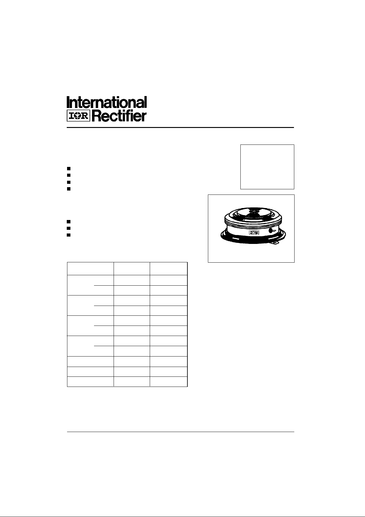
case style TO-200AB (E-PUK)

ST380C..C Series
2222222222222
12
D-368
ELECTRICAL SPECIFICATIONS
Voltage Ratings
Voltage V
DRM/VRRM
, max. repetitive V
RSM
, maximum non- I
DRM/IRRM
max.
Type number Code peak and off-state voltage repetitive peak voltage
@ TJ = TJ max
V V mA
04 400 500
06 600 700
I
T(AV)
Max. average on-state current 960 (440) A 180° conduction, half sine wave
@ Heatsink temperature 55 (75) °C double side (single side) cooled
I
T(RMS)
Max. RMS on-state current 1900 DC @ 25°C heatsink temperature double side cooled
I
TSM
Max. peak, one-cycle 15000 t = 10ms No voltage
non-repetitive surge current 15700 A t = 8.3ms reapplied
12600 t = 10ms 100% V
RRM
13200 t = 8.3ms reapplied Sinusoidal half wave,
I
2
t Maximum I2t for fusing 1130 t = 10ms No voltage Initial TJ = TJ max.
1030 t = 8.3ms reapplied
800 t = 10ms 100% V
RRM
725 t = 8.3ms reapplied
I
2
√t Maximum I2√t for fusing 11300 KA2√s t = 0.1 to 10ms, no voltage reapplied
V
T(TO)
1
Low level value of threshold
voltage
V
T(TO)
2
High level value of threshold
voltage
r
t1
Low level value of on-state
slope resistance
r
t2
High level value of on-state
slope resistance
V
TM
Max. on-state voltage 1.60 V Ipk= 3000A, TJ = TJ max, tp = 10ms sine pulse
I
H
Maximum holding current 600
I
L
Typical latching current 1000
0.85 (16.7% x π x I
T(AV)
< I < π x I
T(AV)
), TJ = TJ max.
0.25 (16.7% x π x I
T(AV)
< I < π x I
T(AV)
), TJ = TJ max.
0.24 (I > π x I
T(AV)
),TJ = TJ max.
Parameter ST380C..C Units Conditions
0.88 (I > π x I
T(AV)
),TJ = TJ max.
On-state Conduction
KA2s
V
mΩ
mA TJ = 25°C, anode supply 12V resistive load
di/dt Max. non-repetitive rate of rise Gate drive 20V, 20Ω, t
r
≤ 1µs
of turned-on current T
J
= TJ max, anode voltage ≤ 80% V
DRM
Gate current 1A, dig/dt = 1A/µs
V
d
= 0.67% V
DRM, TJ
= 25°C
I
TM
= 550A, TJ = TJ max, di/dt = 40A/µs, VR = 50V
dv/dt
= 20V/µs, Gate 0V 100Ω, tp = 500µs
Parameter ST380C..C Units Conditions
Switching
1000 A/µs
t
d
Typical delay time 1.0
t
q
Typical turn-off time 100
µs
ST380C..C 50
 Loading...