

Page 1

Bulletin I25185 rev. B 03/94
ST083S SERIES
INVERTER GRADE THYRISTORS
Features
All diffused design
Center amplifying gate
Guaranteed high dv/dt
Guaranteed high di/dt
High surge current capability
Low thermal impedance
High speed performance
Typical Applications
Inverters
Choppers
Induction heating
All types of force-commutated converters
Major Ratings and Characteristics
Parameters ST083S Units
I
T(AV)
I
T(RMS)
I
TSM
@ T
C
@ 50Hz 2450 A
@ 60Hz 2560 A
85 A
85 °C
135 A
Stud Version
85A
I2t@
V
DRM/VRRM
t
range (*) 10 to 30 µs
q
T
J
(*) tq = 10 to 20µs for 400 to 800V devices
t
= 15 to 30µs for 1000 to 1200V devices
q
50Hz 30 KA2s
@ 60Hz 27 KA
400 to 1200 V
- 40 to 125 °C
www.irf.com
2
s
case style
TO-209AC (TO-94)
1
Page 2

ST083S Series
Bulletin I25185 rev. B 03/94
ELECTRICAL SPECIFICATIONS
Voltage Ratings
Voltage V
DRM/VRRM
Type number Code repetitive peak voltage non-repetitive peak voltage @ T
04 400 500
ST083S 30
08 800 900
10 1000 1100
12 1200 1300
Current Carrying Capability
, maximum V
, maximum I
RSM
DRM/IRRM
VVmA
max.
= TJ max.
J
I
Frequency Units
180
TM
o
el
180oel
I
TM
I
TM
100µs
50Hz 210 120 330 270 2540 1930
400Hz 200 120 350 210 1190 810
1000Hz 150 80 320 190 630 40 0 A
2500Hz 70 25 220 85 250 100
Recovery voltage Vr 50 50 50 50 50 50
Voltage before turn-on Vd V
DRM
V
DRM
V
DRM
Rise of on-state current di/dt 50 50 - - - - A/µs
Case temperature 60 85 60 85 60 85 °C
Equivalent values for RC circuit 22Ω / 0.15µF 22Ω / 0.15µF 22Ω / 0.15µF
On-state Conduction
Parameter ST083S Units Conditions
I
Max. average on-state current 85 A 180° conduction, half sine wave
T(AV)
@ Case temperature 85 °C
Max. RMS on-state current 135 DC @ 77°C case temperature
I
T(RMS)
I
Max. peak, one half cycle, 2450 t = 10ms No voltage
TSM
non-repetitive surge current 2560 A t = 8.3ms reapplied
2060 t = 10ms 100% V
2160 t = 8.3ms reapplied Sinusoidal half wave,
2
I
t Maximum I2t for fusing 30 t = 10ms No voltage Initial TJ = TJ max
27 t = 8.3ms reapplied
21 t = 10ms 100% V
KA2s
19 t = 8.3ms re applied
2
√t Maximum I2√t for fusing 300 KA2√s t = 0.1 to 10ms, no voltage reapplied
I
RRM
RRM
V
2
www.irf.com
Page 3
ST083S Series
Bulletin I25185 rev. B 03/94
On-state Conduction
Parameter ST083S Units Conditions
VTMMax. peak on-state voltage 2.15 ITM= 300A, TJ = TJ max, tp = 10ms sine wave pulse
Low level value of threshold
V
T(TO)1
voltage
High level value of threshold
V
T(TO)2
voltage
Low level value of forward
r
1
t
slope resistance
High level value of forward
r
t2
slope resistance
Maximum holding current 600 TJ = 25°C, IT > 30A
I
H
Typical latching current 1000 TJ = 25°C, VA= 12V, Ra = 6Ω, IG= 1A
I
L
Switching
Parameter ST083S Units Conditions
di/dt Max. non-repetitive rate of rise T
of turned-on current I
t
Typical delay time 0.80
d
t
Max. turn-off time (*) 10 3 0
q
(*) t
= 10 to 20µs for 400 to 800V devices; tq = 15 to 30µs for 1000 to 1200V devices.
q
Blocking
Parameter ST083S Units Conditions
dv/dt Maximum critical rate of rise of T
off-state voltage available on request
Max. peak reverse and off-state
I
RRM
leakage current
I
DRM
1.46 (16.7% x π x I
V
1.52 (I > π x I
2.32 (16.7% x π x I
mΩ
2.34 (I > π x I
mA
= TJ max, V
1000 A/µs
Min Max
500 V/µs
30 mA T
J
= 2 x di/dt
TM
= 25°C, V
T
J
Resistive load, Gate pulse: 10V, 5Ω source
µs
T
= TJ max, I
J
= 50V, tp = 200µs, dv/dt: see table in device code
V
R
= TJ max., linear to 80% V
J
= TJ max, rated V
J
< I < π x I
T(AV)
), TJ = TJ max.
T(AV)
< I < π x I
T(AV)
), TJ = TJ max.
T(AV)
DRM
= rated V
DM
= 100A, commutating di/dt = 10A/µs
TM
= rated V
DRM, ITM
DRM/VRRM
T(AV)
T(AV)
DRM
DRM
applied
), TJ = TJ max.
), TJ = TJ max.
= 50A DC, tp= 1µs
, higher value
Triggering
Parameter ST083S Units Conditions
PGMMaximum peak gate power 40
Maximum average gate power 5
P
G(AV)
I
Max. peak positive gate current 5 A TJ = TJ max, tp ≤ 5ms
GM
+VGMMaximum peak positive
gate voltage
Maximum peak negative
-V
GM
gate voltage
Max. DC gate current required
I
GT
to trigger
V
Max. DC gate voltage required
GT
to trigger
Max. DC gate current not to trigger 20 mA
I
GD
V
Max. DC gate voltage not to trigger 0.25 V
GD
20
5
200 mA
3V
WT
VTJ = TJ max, tp ≤ 5ms
T
TJ = TJ max, rated V
www.irf.com
= TJ max, f = 50Hz, d% = 50
J
= 25°C, VA = 12V, Ra = 6Ω
J
applied
DRM
3
Page 4
ST083S Series
Bulletin I25185 rev. B 03/94
Thermal and Mechanical Specifications
Parameter ST083S Units Conditions
Max. junction operating temperature range -40 to 125
T
J
Max. storage temperature range -40 to 150
T
stg
R
Max. thermal resistance, junction to case 0.195 DC operation
thJC
Max. thermal resistance, case to heatsink 0.08 Mounting surface, smooth, flat and greased
R
thCS
T Mounting torque, ± 10% 15.5 Nm
(137) (Ibf-in)
14 Nm
(120) (Ibf-in)
wt Approximate weight 130 g
Case style TO-209AC (TO-94) See Outline Table
∆R
Conduction
thJC
(The following table shows the increment of thermal resistence R
Conduction angle Sinusoidal conduction Rectangular conduction Units Conditions
180° 0.034 0.025
120° 0.041 0.042
90° 0.052 0.056 K/ W T
60° 0.076 0.079
30° 0.126 0.127
°C
K/W
Non lubricated threads
Lubricated threads
when devices operate at different conduction angles than DC)
thJC
= TJ max.
J
Ordering Information Table
Device Code
1 - Thyristor
2 - Essential part number
3 - 3 = Fast turn off
4 - S = Compression bonding Stud
5 - Voltage code: Code x 100 = V
6 - P = Stud Base 1/2" 20UNF
7 - Reapplied dv/dt code (for tq Test Condition)
8 -tq code
9 - 0 = Eyelet terminals (Gate and Aux. Cathode Leads)
1 = Fast-on terminals (Gate and Aux. Cathode Leads)
2 = Flag terminals (For Cathode and Gate Terminals)
- Critical dv/dt:
10
None = 500V/µsec (Standard value)
L = 1000V/µsec (Special selection)
ST 08 3 S 12 P F K 0
12
34
(See Voltage Ratings Table)
RRM
6
5
7
dv/dt - t
dv/dt (V/µs) 20 50 100 200 400
(µs) 10 CN DN EN FN * HN
t
q
up to 800V
(µs) 15 CL -- -- -- --
t
q
only for
1000/1200V
*Standard part number.
All other types available only on request.
9
8
combinations available
q
12 CM DM EM FM * HM
15 CL DL EL FL HL
18 CP DP EP FP * HP
20 CK DK EK FK * HK
18 CP DP EP FP * --
20 CK DK EK FK * HK
25 CJ DJ EJ FJ HJ
30 -- DH EH FH HH
10
4
www.irf.com
Page 5

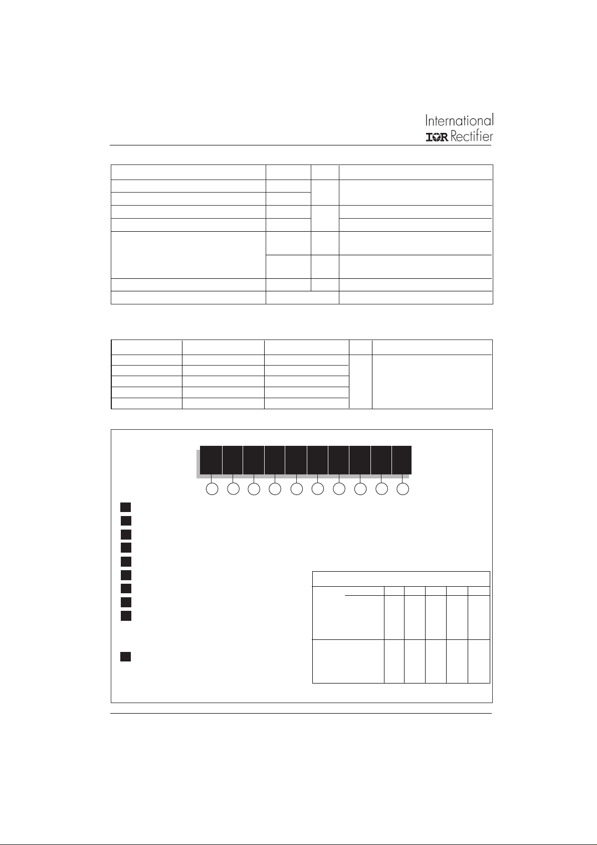
Outline Table
AMP. 280000-1
REF-250
CERAMIC HOUSING
170 (6.69)
157 (6.18)
70 (2.75) MIN.
29 (1.14) MAX.
8.5 (0.33) DIA.
RED SILICON RUBBER
RED CATHODE
RED SHRINK
12.5 (0.49) MAX.
MAX.
21 (0.83)
16.5 (0.65) MAX.
1/2"-20UNF-2A
29.5 (1.16)
MAX.
4.3 (0.17) DIA
C.S. 0.4 mm
(.0006 s.i.)
WHITE GATE
215 (8.46)
WHITE SHRINK
22.5 (0.88) MAX. DIA.
SW 27
FLEXIBLE LEAD
C.S. 16mm
(.025 s.i.)
2
10 (0.39)
ST083S Series
Bulletin I25185 rev. B 03/94
2.6 (0.10) MAX.
2
Case Style TO-209AC (TO-94)
All dimensions in millimeters (inches)
.
N
I
M
)
7
3
.
0
(
.
5
.
N
I
9
M
)
9
7
.
0
(
0
2
Fast-on Terminals
Case Style TO-208AD (TO-83)
All dimensions in millimeters (inches)
www.irf.com
CERAMIC HOUSING
FLAG TERMINALS
46 (1.81)
49 (1.93)
MAX.
12.5 (0.49)
SW 27
22.5 DIA.
(0.89) MAX.
1.5 (0.06) DIA.
10
(0.39)
MAX.
29 (1.14)
MAX.
21(0.83)
29.5 (1.16)
1/2"-20UNF-2A
16.5
2.4 (0.09)
(0.65)
5.2 (0.20) DIA.
7.5
(0.30)
10
(0.39)
5
Page 6

ST083S Series
Bulletin I25185 rev. B 03/94
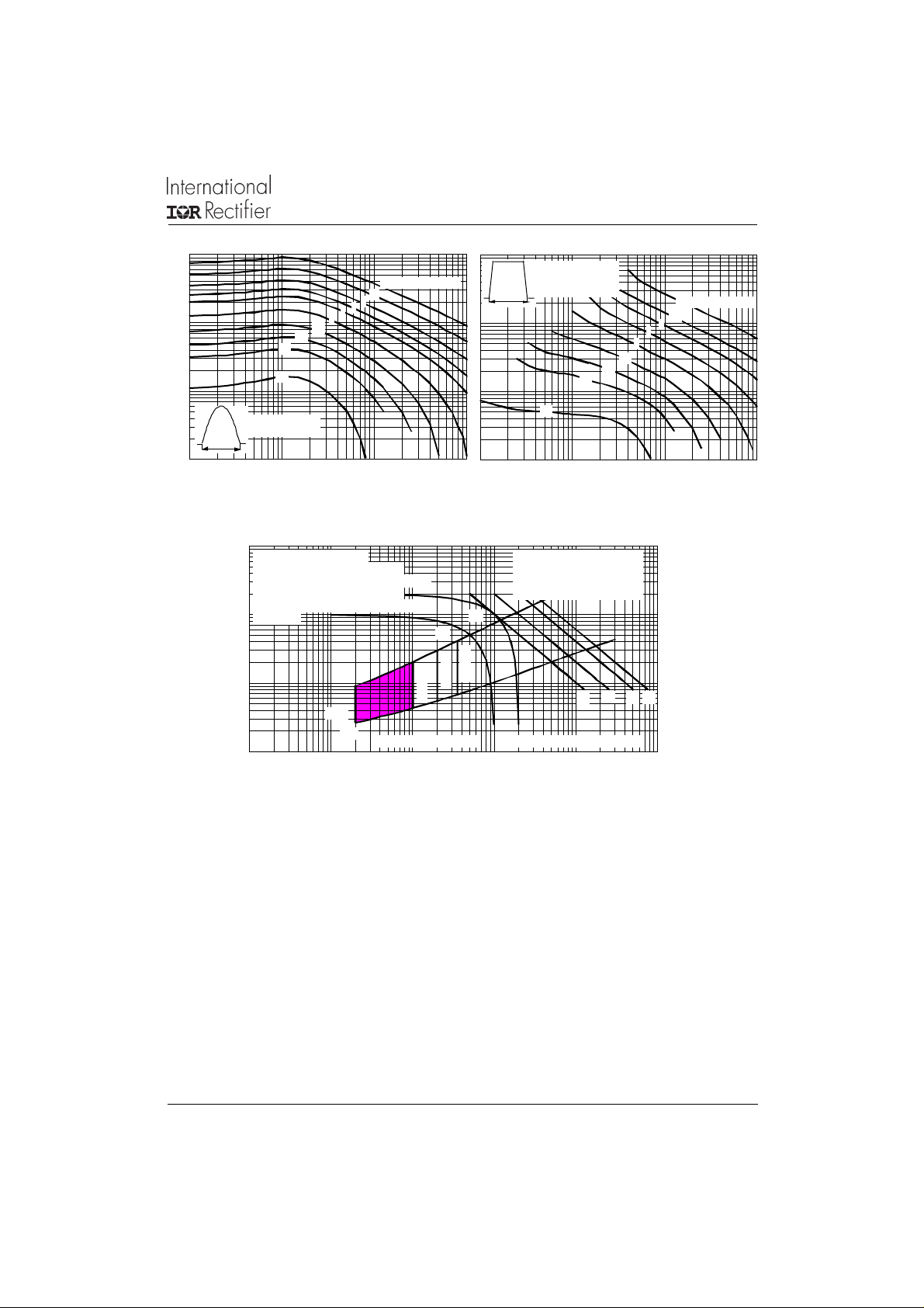
130
ST083S Series
R (DC) = 0.195 K/W
thJC
120
110
Conduction Angle
100
90
80
Maximum Allowable Case Temperature (°C)
0 102030405060708090
30°
60°
90°
Avera g e On- s tate Current (A)
180
160
140
120
100
180°
120°
90°
60°
30°
RMS Limit
80
60
40
20
0
Maximum Average On-state Power Loss (W)
0
10 20 30 40 50 60 70 80 90
Average On-state Current (A)
Fig. 3 - On-state Power Loss Characteristics
120°
180°
Conduction Angl e
ST0 83S Series
T = 125°C
J
130
120
ST08 3 S Se r ies
R (DC) = 0.195 K /W
thJC
110
Conduction Period
100
90
30°
60°
80
90°
120°
70
Maxim um Allowable Case Temper atur e (°C)
0 20406080100120140
Average On-state Current (A)
Fig. 2 - Current Ratings CharacteristicsFig. 1 - Current Ratings Characteristics
0
.3
K/
0
W
.
4
K
/
W
0
.
5
K
/
W
0
.
8
K
/
W
1
.
2
K
/
W
S
A
/
W
=
0
.
1
K
/
W
-
D
e
l
t
a
R
R
0
.
2
t
h
K
25 50 75 100 125
Maximum Allowable Ambient Temperature (°C)
180°
DC
250
200
150
100
50
0
Maximum Average On-state Power Loss (W)
DC
180°
120°
90°
60°
30°
RMS Lim i t
Con ducti on Period
ST0 8 3S Se r ie s
T = 125°C
J
0 20 40 60 80 100 120 140
25 50 75 100 125
Average On-state Current (A)
R
t
h
S
A
=
0
0
.
3
0
.
4
0
.
5
0
.
8
1
2
.
.
2
0
.
K
1
/
W
K
/
W
-
K
/
W
K
/
W
K
/
W
K
/
W
K
/
W
D
e
l
t
a
R
Maximum Allowable Ambient Temperature (°C)
Fig. 4 - On-state Power Loss Characteristics
6
www.irf.com
Page 7

ST083S Series
Bulletin I25185 rev. B 03/94
2200
At Any Rated Load Condit ion A nd W ith
Rated V Applied Fo llowing Surge.
2000
RRM
1800
Initial T = 125°C
J
@ 60 Hz 0.0 083 s
@ 50 Hz 0.0 100 s
1600
1400
1200
ST 083S Series
Peak Half Sine Wave On-state Current ( A)
1000
110100
Number Of Equal Amplitud e Half Cycle Current Pulses (N)
Fig. 5 - Maximum Non-repetitive Surge Current
10000
T = 25°C
J
1000
T = 125°C
J
ST083S Ser ies
Instantaneous On-state Current (A)
100
11.522.533.544.555.566.5
Instantaneous On-state Voltage ( V)
Fig. 7 - On-state Voltage Drop Characteristics
2600
Maximum Non Repetitive Surge Current
2400
2200
2000
Versus Pulse Train Duration. Control
Of Conduction May Not Be Maintained.
Init ia l T = 125 °C
No Voltage Reapplied
Rated V Reapplied
RRM
1800
1600
1400
ST083S Series
1200
Peak Half Sine Wave On-state Current (A)
1000
0.01 0.1 1
Pulse Train Duration (s)
Fig. 6 - Maximum Non-repetitive Surge Current
1
Steady State Value
R = 0.195 K/W
thJC
thJC
(DC Operation)
0.1
ST 083S Series
0. 01
Transient Thermal Impedance Z (K/W)
0.001 0.01 0.1 1 10
Square Wave Pulse Duration (s)
Fig. 8 - Thermal Impedance Z
Characteristic
thJC
J
160
140
120
100
80
ST083S Series
T = 125 °C
J
I = 500 A
TM
300 A
200 A
100 A
120
110
100
90
80
70
60
50
60
40
20
10 20 30 40 50 60 70 80 90 100
Maximum Rever se Re cov ery Charge - Qrr (µC)
Rate Of Fall Of On-state Current - di/dt (A/µs)
50 A
40
30
20
10
Maximum Reverse Reco very Current - Irr (A)
10 20 30 40 50 60 70 80 90 100
ST083S Ser ies
T = 125 °C
J
Rate Of Fall Of Forward Current - di/dt (A/µs)
Fig. 9 - Reverse Recovered Charge Characteristics Fig. 10 - Reverse Recovery Current Characteristics
www.irf.com
I = 500 A
TM
300 A
200 A
100 A
50 A
7
Page 8

ST083S Series
Bulletin I25185 rev. B 03/94
1E4
Snu bber circuit
R = 22 ohms
s
C = 0.15 µF
s
V = 80% V
D
1E3
500
tp
400
ST083S Series
Si nu s o idal pu lse
T = 60°C
C
1000
1500
2000
2500
1E2
3000
Peak On-state Current (A)
1E1
1E1 1E 2 1E3 1E 4
100
200
Pulse Basewidth (µs)
Fig. 11 - Frequency Characteristics
1E4
Snubber circuit
R = 22 ohms
s
C = 0.15 µF
s
V = 80% V
D
1E3
100
200
400
500
1000
1500
3000
2500
2000
ST083S Series
Trapezoidal pulse
T = 60°C
tp
di/dt = 50A/µs
C
1E2
Pe ak On-s ta t e Current (A )
1E1
1E1 1E2 1E3 1E4
Pulse Basewidth (µs)
Fig. 12 - Frequency Characteristics
DRM
50 Hz
2000
2500
3000
1E1 1E2 1E3 1E4
1E1
1E4
1500
1000
500
tp
200
400
ST083S Series
Sinusoid al pulse
T = 85°C
C
Pu ls e Ba s ewid th (µs)
ST08 3S Se ries
Trapezoidal pulse
T = 85°C
C
tp
2000
2500
di/dt = 50A/µs
1000
1500
500
400
200
DRM
50 H z
1E4
1E1
1E1 1E2 1E3 1E4
Pulse Basewidth (µs)
Snubber circuit
R = 22 ohms
s
s
C = 0.15 µF
D
V = 80% V
Snu bber circuit
R = 22 ohms
C = 0.15 µF
V = 80% V
DRM
50 H z
100
s
s
D
DRM
50 Hz
100
1E4
Snubber circuit
R = 22 ohms
s
s
C = 0.15 µF
V = 80% V
D
1E3
100
200
400
500
1000
1500
3000
2500
2000
ST083S Series
Trapezoidal pulse
T = 60°C
tp
di/dt = 100A/µs
C
1E2
Peak On- s tate Curr ent (A)
1E1
1E1 1E2 1E3 1E4
Puls e Base width (µs)
Fig. 13 - Frequency Characteristics
8
ST083S Series
Trapezoidal pulse
T = 85°C
C
DRM
50 Hz
1E4
tp
di/dt = 100A/µs
200
400
500
1000
1500
2000
2500
1E1 1 E2 1E3 1E4
1E1
Pu lse Ba s e w idth (µs)
Snu bber circuit
R = 22 ohms
s
C = 0.15 µF
s
V = 80% V
D
DRM
50 H z
100
www.irf.com
Page 9
ST083S Series
Bulletin I25185 rev. B 03/94
1E4
20 joules per pulse
10
5
3
2
1E3
0.2
0.1
0.3
0.5
1
1E2
Peak On-state Current (A)
1E1
1E11E21E31E4
tp
ST083S Series
Sin usoid al pulse
1E1 1E2 1E3 1E4
1E1
1E4
Pulse Basewidth (µs)
Fig. 14 - Maximum On-state Energy Power Loss Characteristics
100
Rectangular gate pulse
a) Reco mmended load line for
rated di/dt : 20V, 10ohms; tr<=1 µs
b) Recommended load line for
<=30% rated di/dt : 10V, 10ohms
10
tr<=1 µs
Tj=125 °C
(b)
(a)
Tj= - 40 °C
Tj=25 °C
1
Instantaneous Gate Voltage (V)
0.1
0.001 0.01 0.1 1 1 0 100
VGD
IGD
Device : ST083S Se ries
Frequency Limited by PG(AV)
Instantaneous Gate Current (A)
Fig. 15 - Gate Characteristics
ST083S Series
Rectangular pulse
di/dt = 50A/µs
tp
0.3
0.2
0.1
Pu ls e Base w idth (µs)
(1) PGM = 10W, tp = 20ms
(2) PGM = 20W, tp = 10ms
(3) PGM = 40W, tp = 5ms
(4) PGM = 60W, tp = 3.3ms
(2)
(1)
0.5
(3)
4
2
1
(4)
20 joules per pulse
7.5
www.irf.com
9
 Loading...