

Datasheet SD603C10S10C, SD603C12S15C, SD603C14S15C, SD603C16S15C, SD603C20S20C Datasheet (International Rectifier)
...
Bulletin I2068/B
Next Data SheetIndex
Previous Datasheet
To Order
SD603C..C SERIES
FAST RECOVERY DIODES
Features
High power FAST recovery diode series
1.0 to 2.0 µs recovery time
High voltage ratings up to 2200V
High current capability
Optimized turn on and turn off characteristics
Low forward recovery
Fast and soft reverse recovery
Press-puk encapsulation
Case style conform to JEDEC B-43
Maximum junction temperature 125°C
Typical Applications
Snubber diode for GTO
High voltage free-wheeling diode
Fast recovery rectifier applications
Major Ratings and Characteristics
Parameters SD603C..C Units
I
F(AV)
@ T
hs
I
F(RMS)
@ T
hs
I
FSM
2
I
t @ 50Hz 346 KA2s
@ 50Hz 8320 A
@ 60Hz 8715 A
@ 60Hz 316 KA
600 A
55 °C
942 A
25 °C
Hockey Puk Version
600A
case style B-43
2
s
V
range 400 to 2200 V
RRM
t
range 1.0 to 2.0 µs
rr
T
J
@ T
J
25 °C
- 40 to 125 °C
D-707
SD603C..C Series
Next Data SheetIndex
Previous Datasheet
To Order
ELECTRICAL SPECIFICATIONS
Voltage Ratings
Voltage V
Type number Code peak and off-state voltage repetitive peak voltage T
04 400 500
SD603C..S10C 08 800 900
10 1000 1100
12 1200 1300
SD603C..S15C 14 1400 1500
16 1600 1700
SD603C..S20C
20 2000 2100
22 2200 2300
Forward Conduction
Parameter SD603C..C Units Conditions
Max. average forward current 600(300) A 180° conduction, half sine wave.
I
F(AV)
@ Heatsink temperature 55(75) °C Double side (single side) cooled
I
Max. RMS current 942 A @ 25°C heatsink temperature double side cooled
F(RMS)
I
Max. peak, one-cycle 8320 t = 10ms No voltage
FSM
non-repetitive forward current 8715 t = 8.3ms reapplied
2
I
t Maximum I2t for fusing 346 t = 10ms No voltage Initial TJ = TJ max.
2
I
√t Maximum I2√t for fusing 3460 KA2√s t = 0.1 to 10ms, no voltage reapplied
V
Low level of threshold voltage 1.36 (16.7% x π x I
F(TO)1
V
High level of threshold voltage 1.81 (I > π x I
F(TO)
2
r
Low level of forward slope resistance 0.87 (16.7% x π x I
f1
r
High level of forward slope resistance 0.67 (I > π x I
f2
V
Max. forward voltage 2.97 V Ipk= 1885A, TJ = 25°C, tp = 10ms sinusoidal wave
FM
max. repetitive V
RRM
, maximum non- I
RSM
V V mA
7000 t = 10ms 100% V
7330 t = 8.3ms reapplied Sinusoidal half wave,
316 t = 8.3ms reapplied
245 t = 10ms 100% V
224 t = 8.3ms reapplied
A
KA2s
V
mΩ
F(AV)
), TJ = TJ max.
F(AV)
F(AV)
), TJ = TJ max.
F(AV)
RRM
RRM
< I < π x I
< I < π x I
), TJ = TJ max.
F(AV)
), TJ = TJ max.
F(AV)
2222222222222
max.
RRM
= 125°C
J
45
12
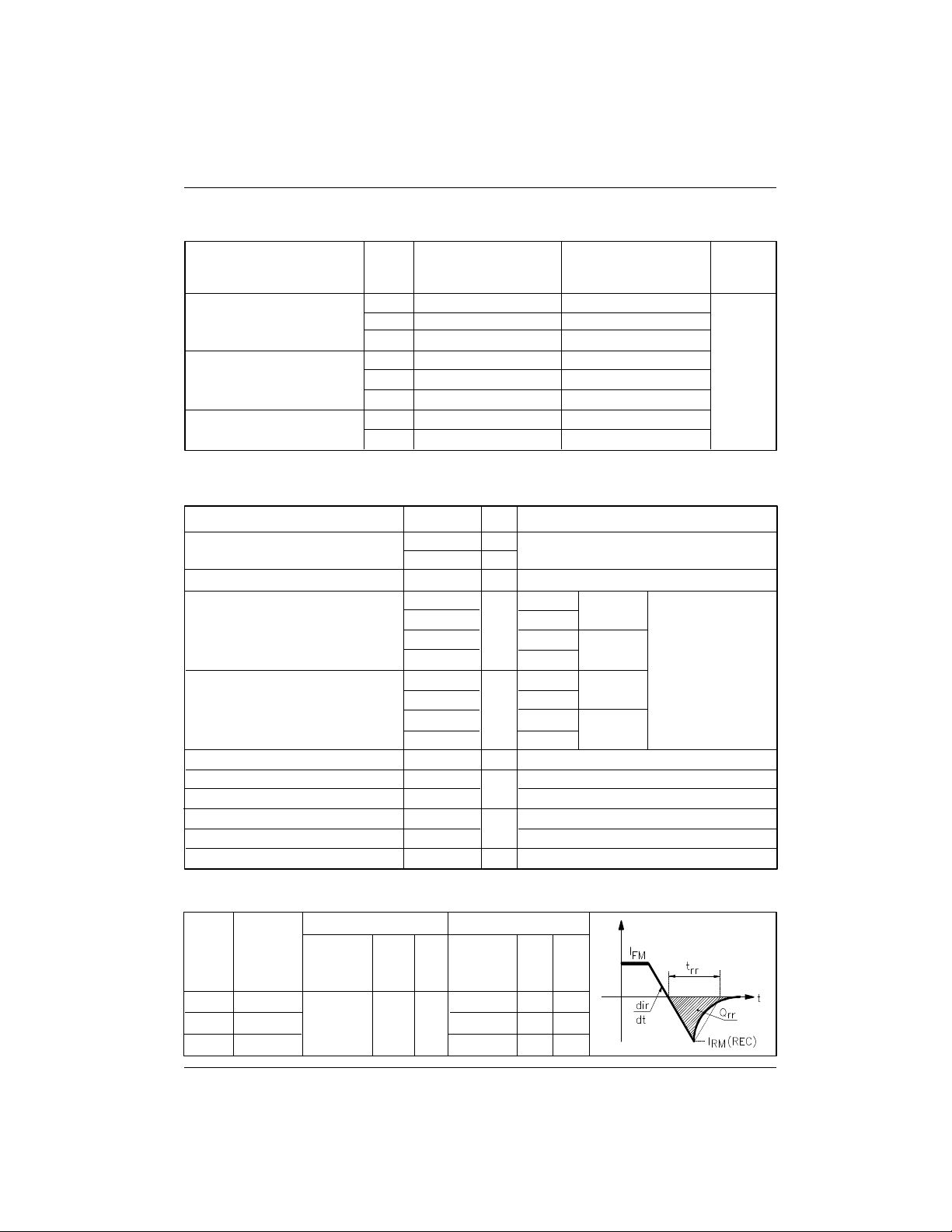
Recovery Characteristics
Code
S10 1.0 2.0 45 34
S15 1.5 1000 25 -30 3.2 87 51
S20 2.0 3.5 97 55
T
= 25 oC
J
typical t
@ 25% I
rr
RRM
Test conditions Max. values @ T
I
pk
Square Pulse @ 25% I
di/dt V
r
t
rr
RRM
(µs) (A) (A/µs) (V) (µs) (µC) (A)
D-708
= 125 °C
J
QrrI
rr
SD603C..C Series
To Order
Next Data SheetIndex
Previous Datasheet
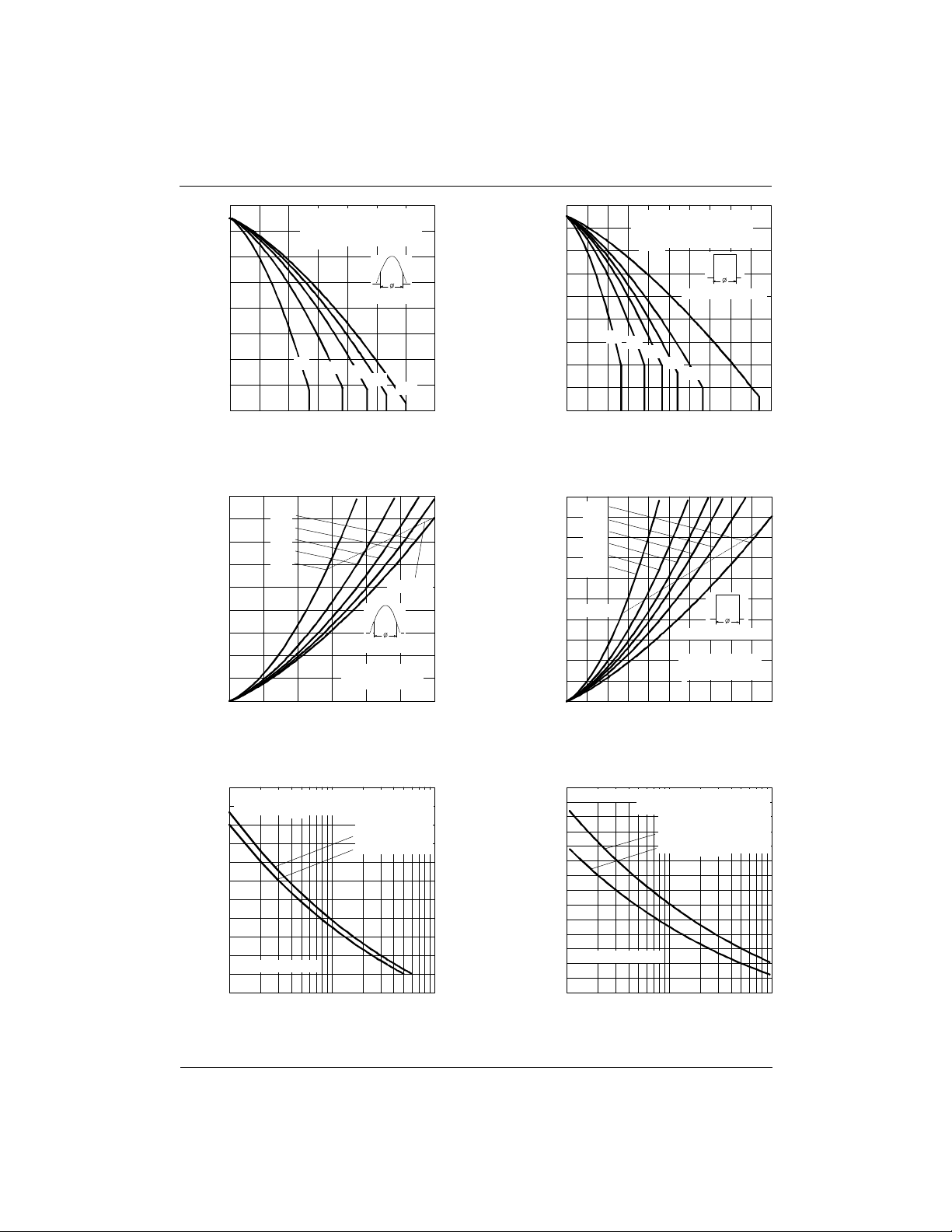
Fig. 3 - Current Ratings Characteristics
Fig. 5 - Forward Power Loss Characteristics Fig. 6 - Forward Power Loss Characteristics
Fig. 4 - Current Ratings Characteristics
Fig. 7 - Maximum Non-repetitive Surge Current
Single and Double Side Cooled
D-711
Fig. 8 - Maximum Non-repetitive Surge Current
Single and Double Side Cooled

SD603C..C Series
To Order
Next Data SheetIndex
Previous Datasheet
Fig. 9 - Forward Voltage Drop Characteristics
Fig. 11 - Typical Forward Recovery Characteristics
Fig. 10 - Thermal Impedance Z
Characteristic
thJ-hs
Fig. 14 - Recovery Current CharacteristicsFig. 12 - Recovery Time Characteristics Fig. 13 - Recovery Charge Characteristics
D-712

SD603C..C Series
To Order
Next Data SheetIndex
Previous Datasheet
Fig. 15 - Recovery Time Characteristics
Fig. 18 - Recovery Time Characteristics Fig. 19 - Recovery Charge Characteristics Fig. 20 - Recovery Current Characteristics
Fig. 17 - Recovery Current CharacteristicsFig. 16 - Recovery Charge Characteristics
Fig. 21 - Maximum Total Energy Loss Per Pulse Characteristics
D-713

SD603C..C Series
To Order
Next Data SheetIndex
Previous Datasheet
Fig. 22 - Maximum Total Energy Loss Per Pulse Characteristics
Fig. 23 - Maximum Total Energy Loss Per Pulse Characteristics
D-714

Thermal and Mechanical Specifications
To Order
Next Data SheetIndex
Previous Datasheet
Parameter SD603C..C Units Conditions
TJMax. operating temperature range -40 to 125
T
Max. storage temperature range -40 to 150
stg
R
Max. thermal resistance, 0.076 DC operation single side cooled
thJ-hs
junction to heatsink 0.038 DC operation double side cooled
F Mounting force, ± 10% 9800 N
(1000) (Kg)
wt Approximate weight 83 g
Case style B-43 See Outline Table
Conduction
∆R
thJ-hs
(The following table shows the increment of thermal resistence R
Conduction angle Units Conditions
180° 0.006 0.007 0.005 0.005
120° 0.008 0.008 0.008 0.008
90° 0.010 0.010 0.011 0.011 K/W T
60° 0.015 0.015 0.016 0.015
30° 0.026 0.025 0.026 0.025
Sinusoidal conduction Rectangular conduction
Single Side Double Side Single Side Double Side
°C
K/W
when devices operate at different conduction angles than DC)
thJ-hs
J
SD603C..C Series
23
= TJ max.
Ordering Information Table
Device Code
1 - Diode
2 - Essential part number
3 - 3 = Fast recovery
4 - C = Ceramic Puk
5 - Voltage code: Code x 100 = V
6 - t
7 - C = Puk Case B-43
code (see Recovery Characteristics table)
rr
SD 60 3 C 22 S20 C
3
(see Voltage Ratings table)
RRM
51 2
4
6
D-7093333
7

SD603C..C Series
14.4 (0.57)
15.4 (0.61)
42 (1.65) D IA. M A X .
To Order
Next Data SheetIndex
Previous Datasheet
Outline Table
3.5 (0.14) DIA. NOM. x
1.8 (0.07) DEEP MIN. BOTH ENDS
Conform to JEDEC B-43
All dimensions in millimeters (inches)
0.8(0.03) MIN.
BOTH ENDS
12
25.3 (1) DIA. MAX.
TWO PLACES
40.5 (1.59) DIA. MAX.
2222222222222
Fig. 1 - Current Ratings Characteristics Fig. 2 - Current Ratings Characteristics
D-710
 Loading...