International Rectifier PVT422P, PVT422P-T Datasheet

PD 1.043
PVT422P
Microelectronic
Power IC Relay
Dual Pole, Normally Open 0-400V, 120mA AC/DC
(HEXFET is the registered trademark for International Rectifier Power MOSFETs)
General Description
The PVT422P Series Photovoltaic Relay is a dualpole, normally open solid-state relay that can
replace electromechanical relays in many applications. It utilizes International Rectifier’s HEXFET
power MOSFET as the output switch, dr iven by an
integrated circuit photovoltaic generator of novel
construction. The output switch is controlled by
radiation from a GaAiAs light emitting diode (LED)
which is optically isolated from the photovoltaic
generator.
PVT422P is ideally suited for PCMCIA card
applications. Its extremely low profile allows it to be
used in Type II cards whose outer shells are only
5mm thick.
Series PVT422P Relays are packaged in an 8-pin,
molded ‘Thin-Pak’ DIP package with ‘gull-wing’
surface mount terminals. It is available in plastic
shipping tubes or on tape-and-reel. Please refer t o
Par t Identification (opposite) for details.
PVT422P Features
HEXFET Power MOSFET output
■■
■■
■
Bounce-free operation
■■
■■
■
3,750 V
RMS
I/O isolation
■■
■■
■
Linear AC/DC operation
■■
■■
■
Solid-State reliability
■■
■■
■
UL recognized
■■
■■
■
PVT422P
‘Thin-Pak’
Applications
On/Off Hook switch
■■
■■
■
Dial-Out relay
■■
■■
■
Ring injection relay
■■
■■
■
General switching
■■
■■
■
Part Identification
PVT422P surface-mount, plastic shipping tube
PVT422P-T surface-mount, tape-and-reel
HEXFET® Power MOSFET Photovoltaic Relay

2
Series PVT422P HEXFET® Photovoltaic Relay
INPUT CHARACTERISTICS Limits Units
Minimum Control Current (See figure1) 2.0 mA
Maximum Control Current for Off-State Resistance @TA=+25°C 0.4 mA
Control Current Range (Caution: current limit input LED, see figure 5) 2.0 to 25 mA
Maximum Reverse Voltage 7.0 V
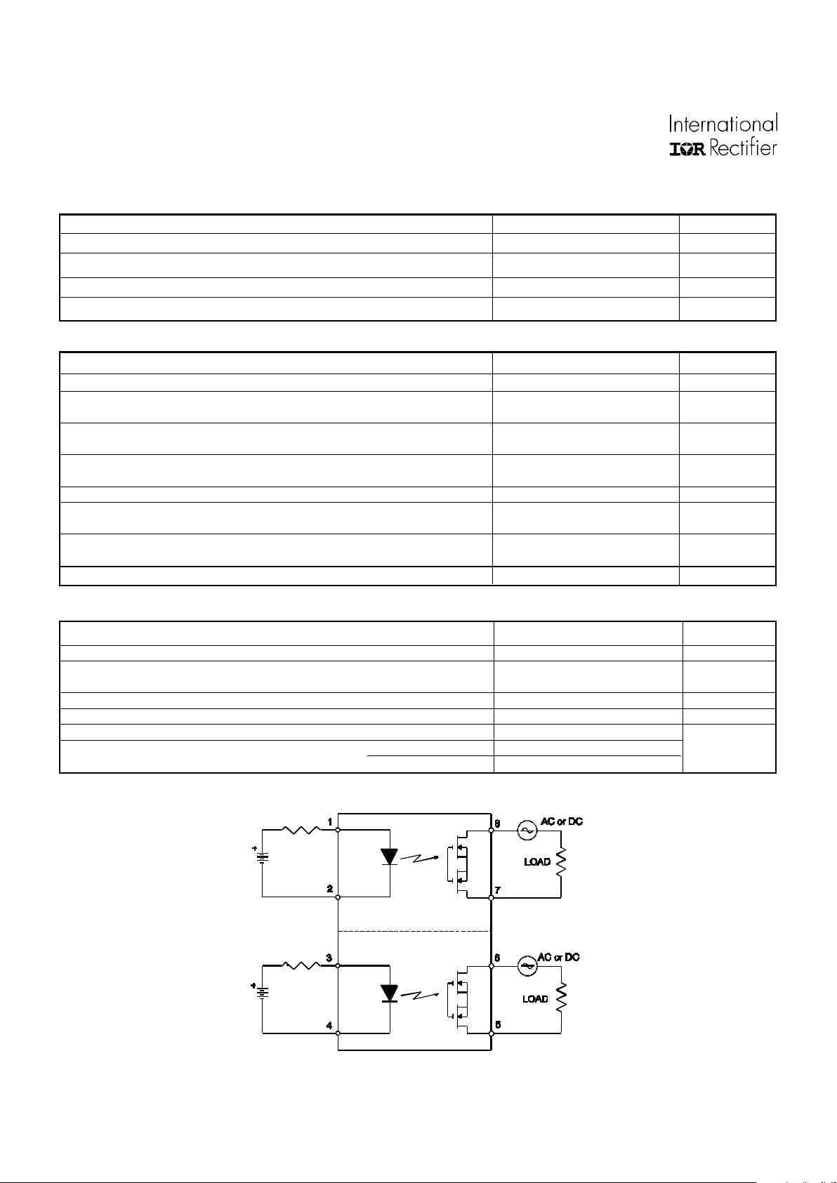
Connection Diagram
OUTPUT CHARACTERISTICS Limits Units
Operating Voltage Range 0 to ±400 V
(DC or AC peak)
Maximum Load Current @ TA=+40°C
5mA Control (See figure 1) (single and dual channel operation) 120 mA
Maximum Peak Load Current (10ms maximum duration)
(single and dual channel operation) 350 mA
Maximum On-State Resistance @T
A
=+25°C
For 50mA Pulsed load, 5mA Control (see figure3) 35 Ω
Maximum Off-State Leakage @TA=+25°C, ±320V (see figure 4) 1.0 µA
Maximum Turn-On Time @T
A
=+25°C (see figure 6) 2.0 ms
For 50mA, 100 VDC load, 5mA Control
Maximum Turn-Off Time @T
A
=+25°C (see figure 6) 2.0 ms
For 50mA, 100 VDC load, 5mA Control
Maximum Output Capacitance @ 50V
DC
12 pF
GENERAL CHARACTERISTICS Limits Units
Minimum Dielectric Strength, Input-Output 4000 V
RMS
Minimum Dielectric Strength, Pole-to-Pole 1000 V
DC
Minimum Insulation Resistance, Input-Output, @TA=+25°C, 50%RH, 100V
DC
10
12
Ω
Maximum Capacitance, Input-Output 1.0 pF
Maximum Pin Soldering Temperature (10 seconds maximum) +260
Ambient Temperature Range: Operating -40 to +85 °C
Storage -40 to +100
Electrical Specifications (-40°C ≤ TA ≤ +85°C unless otherwise specified)
 Loading...