International Rectifier IRLR 8103 V Service Manual

www.DataSheet4U.com
• N-Channel Application-Specific MOSFETs
S
D
G
DS(on)
7.9 m
SW
Absolute Maximum Ratings
V
Continuous Drain or Source Current
I
Thermal Resistance
• Ideal for CPU Core DC-DC Converters
• Low Conduction Losses
• Low Switching Losses
• Minimizes Parallel MOSFETs for high current
applications
•
100% RG Tested
Description
This new device employs advanced HEXFET Power
MOSFET technology to achieve an unprecedented
balance of on-resistance and gate charge. The reduced
conduction and switching losses make it ideal for high
efficiency DC-DC converters that power the latest
generation of microprocessors.
The IRLR8103V has been optimized for all parameters
that are critical in synchronous buck converters including
R
, gate charge and Cdv/dt-induced turn-on immunity.
DS(on)
The IRLR8103V offers an extremely low combination of
Qsw & R
synchronous FET applications.
for reduced losses in both control and
DS(on)
The package is designed for vapor phase, infra-red,
convection, or wave soldering techniques. Power
dissipation of greater than 2W is possible in a typical
PCB mount application.
PD-94021C
IRLR8103V
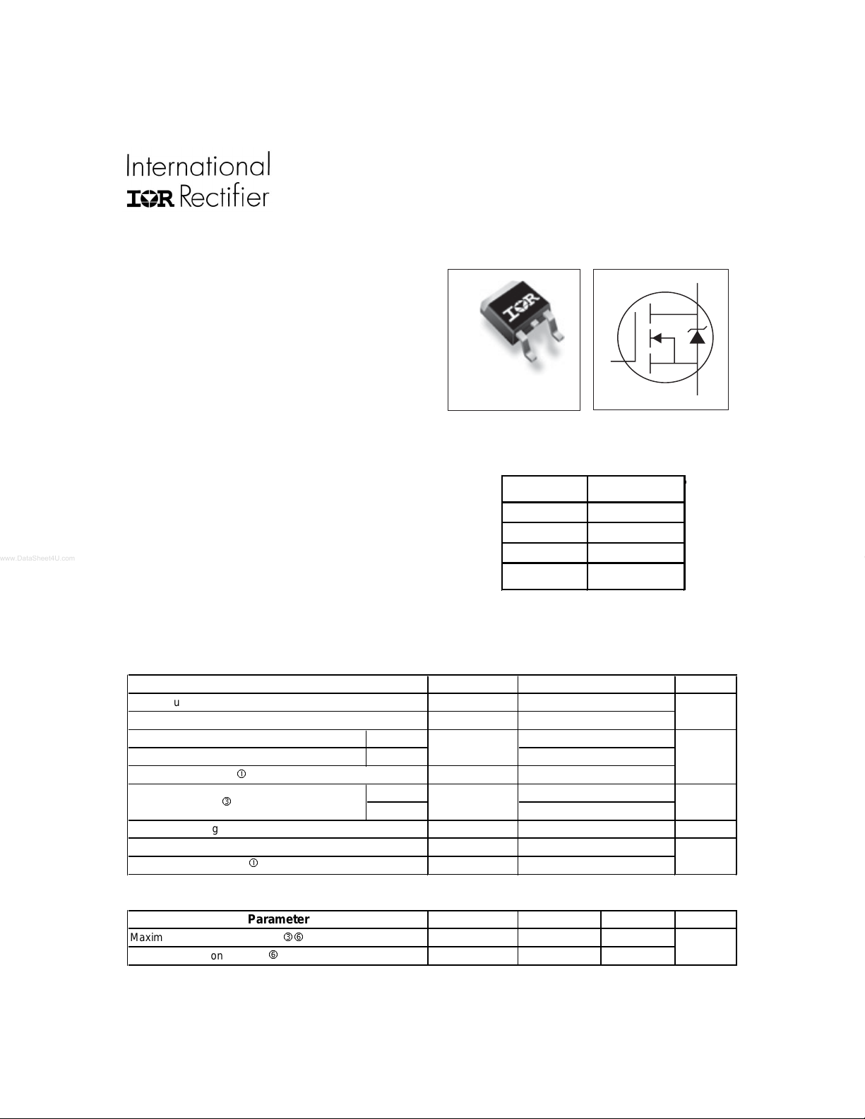
D-Pak
DEVICE CHARACTERISTICS
IRLR8103V
R
Q
G
Q
Q
OSS
Ω
27 nC
12 nC
29nC
Parameter
Drain-Source Volt age
Gate-Source Voltage
(V
> 10V)
GS
Pulsed Drain Current
Power Dissip ation
Junction & Storage Temperature Range
Continuous Source Current (Body Diode)
Pulsed Source Current
c
e
c
Parameter
Maximum Ju nct ion-to -Am bie nt
Maximum Ju nct ion-to-Case
eh
h
TC = 25°C
TC= 90°C
TC = 25°C
TC = 90°C
Symbol Units
DS
V
GS
I
D
I
DM
P
D
T
, T
J
STG
I
S
SM
Symbol Typ. Max. Units
R
θJA
R
θJC
IRLR8103V
30
±20
91
63
363
115
60
-55 to 150
91
363
––– 50
––– 1.09
V
A
W
°C
A
°C/W
www.irf.com 1
10/22/04

IRLR8103V
Electrical Charact eristics
Source-Drain Rating & Characteristics
–––
0.9
1.3
V
Reverse Recovery Charge
Parameter Symbol Min Typ Max Units
Drain-to-Source Breakdown Voltage
Static Drain-Source
On-Resistance ––– 7.9 10.5
Gate Threshold Voltage
Drain-to-Source Leakage Current
Gate-Source Leakage Current
Total Gate Charge, Control FET
Total Gate Charge, Synch FET
Pre-Vth Gate-Source Charge
Post-Vth Gate-Source Charge
Gate to Drain Charge
Switch Charge (Q
+ Qgd)Q
gs2
Output Charge
Gate Resistance
Turn-On Delay Time
Rise Time
Turn-Off Delay Time
Fall Time
Input Capacitance
Output Capacitance
Reverse Transfer Capacitance
BV
R
V
I
DSS
I
GSS
Q
Q
Q
Q
Q
Q
R
t
d(on)
t
r
t
d(off)
t
f
C
C
C
DSS
DS(on)
GS(th)
G
G
GS1
GS2
GD
SW
OSS
G
iss
oss
rss
30 ––– ––– V
––– 6.9 9.0
1.0 ––– 3.0 V
––– ––– 50 µA
––– ––– 20
––– ––– 100
––– ––– ±100 nA
––– 27 –––
––– 23 –––
––– 4.7 –––
––– 2.0 –––
––– 9.7 –––
––– 12 –––
––– 29 –––
0.8 ––– 3.1
––– 10 –––
––– 9 –––
––– 24 –––
––– 18 –––
––– 2672 –––
––– 1064 –––
––– 109 –––
Conditions
VGS = 0V, ID = 250µA
= 10V, ID = 15A
V
GS
Ω
m
V
= 4.5V, ID = 15A
GS
V
= VGS, ID = 250µA
DS
= 30V, VGS = 0V
V
DS
= 24V, VGS = 0
V
DS
µA
V
= 24V, VGS = 0, TJ = 100°C
DS
V
= ± 20V
GS
VGS = 5V, ID = 15A, VDS = 16V
V
= 5V, VDS < 100mV
GS
nC
V
= 16V, ID = 15A
DS
= 16V, VGS = 0
V
DS
Ω
V
= 16V
DD
= 15A
I
D
ns
pF
= 5.0V
V
GS
Clamped Inductive Load
= 16V, VGS=0
V
GS
d
d
Parameter Symbol Min Typ Max Units
Diode Forward Voltage
Reverse Recovery Charge
(with Parallel Schottky)
f
Notes:
Repetitive rating; pulse width limited by max. junction temperature.
Pulse width ≤ 400 µs; duty cycle ≤ 2%.
When mounted on 1 inch square copper board, t < 10 sec.
Typ = measured - Q
Typical values of RDS(on) measured at VGS = 4.5V, QG, QSW and Q
R
is measured at TJ approximately 90°C
θ
Conditions
d
, V
V
SD
f
oss
Q
rr
Q
rr(s)
––– 103 ––– nC
––– 96 ––– nC
measured at VGS = 5.0V, IF = 15A.
OSS
IS = 15A
di/dt ~ 700A/µs
= 16V, VGS = 0V, IF = 15A
V
DS
di/dt = 700A/µs , (with 10BQ040)
= 16V, VGS = 0V, IF = 15A
V
DS
GS
= 0V
www.irf.com2

IRLR8103V
1000
100
TOP
BOTTOM
VGS
15V
10V
7.0V
5.5V
4.5V
4.0V
3.5V
2.7V
2.7V
10
D
I , Drain-to-Source Current (A)
20µs PULSE WIDTH
°
T = 25 C
1
0.1 1 10 100
V , Drain-to-Sou rce Voltage (V)
DS
1000
J
1000
100
TOP
BOTTOM
VGS
15V
10V
7.0V
5.5V
4.5V
4.0V
3.5V
2.7V
2.7V
10
D
I , Drain-to-Source Current (A)
20µs PULSE WIDTH
°
T = 150 C
1
0.1 1 10 100
V , Drain-to-Source Voltage (V)
DS
J
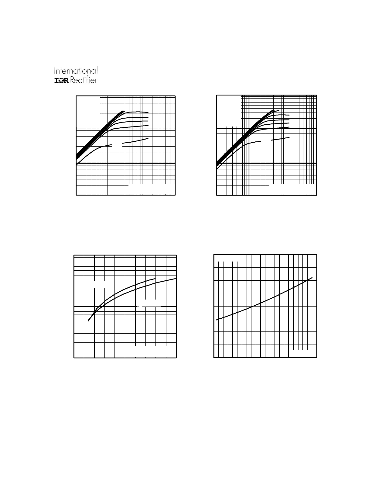
Fig 2. Typical Output CharacteristicsFig 1. Typical Output Characteristics
2.0
I =
D
15A
1.5
1.0
100
°
T = 25 C
J
°
T = 150 C
J
(Normalized)
0.5
D
I , Drain-to-Source Current (A)
V = 15V
DS
10
2.0 3.0 4.0 5.0 6.0 7.0
V , Gate-to-Source Voltage (V)
GS
20µs PULSE WIDTH
Fig 3. Typical Transfer Characteristics
DS(on)
R , Drain-to-Source On Resistance
0.0
-60 -40 -20 0 20 40 60 80 100 120 140 160
T , Junction Te m peratur e ( C)
J
Fig 4. Normalized On-Resistance
V =
GS
°
10V
Vs. Temperature
www .irf.com 3
 Loading...