

International Rectifier IRHNA9064 Datasheet
Provisional Data Sheet No. PD-9.1447
Next Data SheetIndex
Previous Datasheet
To Order
REPETITIVE AVALANCHE AND dv/dt RATED IRHNA9064
®
HEXFET
TRANSISTOR
P-CHANNEL
RAD HARD
-60V olt,
0.055Ω0.055Ω
0.055Ω, RAD HARD HEXFET
0.055Ω0.055Ω
International Rectifier’s P-Channel RAD HARD technology
HEXFETs demonstrate excellent threshold v oltage stability
and breakdown voltage stability at total radiation doses as
high as 10
5
Rads (Si). Under identical pre- and post-radiation test conditions, International Rectifier’s P-Channel RAD
HARD HEXFETs retain identical electrical specifications up
5
to 1 x 10
circuitry is required. These devices are also capable of surviving transient ionization pulses as high as 1 x 10
Rads (Si) total dose. No compensation in gate drive
12
Rads
(Si)/Sec, and return to normal operation within a few microseconds. Single Event Effect (SEE) testing of International
Rectifier P-Channel RAD HARD HEXFETs has demonstrated virtual immunity to SEE failure. Since the P-Channel RAD HARD process utilizes International Rectifier’s
patented HEXFET technology , the user can expect the highest quality and reliability in the industry.
P-Channel RAD HARD HEXFET transistors also feature
all of the well-established advantages of MOSFETs, such
Product Summary
Part Number BVDSS RDS(on) ID
IRHNA9064 -60V 0.055Ω -48A
Features:
n Radiation Hardened up to 1 x 10
n Single Event Burnout (SEB) Hardened
n Single Event Gate Rupture (SEGR) Hardened
n Gamma Dot (Flash X-Ray) Hardened
n Neutron Tolerant
n Identical Pre- and Post-Electrical Test Conditions
n Repetitive Avalanche Rating
n Dynamic dv/dt Rating
n Simple Drive Requirements
n Ease of Paralleling
n Hermetically Sealed
n Surface Mount
n Light-Weight
as voltage control, very fast switching, ease of paralleling
and temperature stability of the electrical parameters. They
are well-suited for applications such as switching power
supplies, motor controls, inverters, choppers, audio amplifiers and high-energy pulse circuits in space and weapons
environments.
Absolute Maximum Ratings
Parameter IRHNA9064 Units
ID @ VGS = -12V, TC = 25°C Continuous Drain Current -48
ID @ VGS = -12V, TC = 100°C Continuous Drain Current -30
I
DM
PD @ TC = 25°C Max. Power Dissipation 300 W
V
GS
E
AS
I
AR
E
AR
dv/dt Peak Diode Recovery dv/dt -5.5
T
J
T
STG
Pulsed Drain Current -192
Linear Derating Factor 2.4 W/K
Gate-to-Source Voltage ± 20 V
Single Pulse Avalanche Energy 500 mJ
Avalanche Current -48 A
Repetitive Avalanche Energy 30 mJ
Operating Junction -55 to 150
Storage Temperature Range
Package Mounting Surface Temperature
Weight 3.3 (typical) g
300 (For 5 sec)
5
Rads (Si)
Pre-Radiation
A
V/ns
o
C
IRHNA9064 Pre-Radiation
Next Data SheetIndex
Previous Datasheet
To Order
Electrical Characteristics @ Tj = 25°C (Unless Otherwise Specified)
Parameter Min Typ Max Units Test Conditions
BV
DSS
∆BV
R
DS(on)
V
GS(th)
g
fs
I
DSS
I
GSS
I
GSS
Q
g
Q
gs
Q
gd
t
(on)
d
t
r
t
(off)
d
t
f
L
D
L
S
DSS
Drain-to-Source Breakdown Voltage -60 — — V VGS =0 V, ID = -1.0mA
/∆TJTemperature Coefficient of Breakdown — -0.048 — V/°C Reference to 25°C, ID = -1.0mA
Voltage
Static Drain-to-Source — — 0.055 VGS = -12V, ID = -30A
On-State Resistance — — 0.065
Gate Threshold Voltage -2.0 — -4.0 V VDS = VGS, ID = -1.0mA
Forward Transconductance 16 — — S ( )VDS > -15V, IDS = -30A
Zero Gate Voltage Drain Current — — -25 VDS= 0.8 x Max Rating,VGS=0V
— — -250 VDS = 0.8 x Max Rating
Gate-to-Source Leakage Forward — — -100 VGS =-20 V
Gate-to-Source Leakage Reverse — — 100 VGS = 20V
Total Gate Charge — — 260 VGS = -12V, ID = -48A
Gate-to-Source Charge — — 60 nC VDS = Max Rating x 0.5
Gate-to-Drain (‘Miller’) Charge — — 86
Turn-On Delay Time — — 62 VDD = -30V , ID = -48A,
Rise Time — — 227 RG = 2.35Ω
Turn-Off Delay Time — — 2 00
Fall Time — — 115
Internal Drain Inductance — 8.7 —
Internal Source Inductance — 8.7 —
Ω
Ω
µA
nA
ns
Measured from drain lead,
6mm (0.25 in) from package
to center of die.
nH
Measured from source lead,
6mm (0.25 in) from package
to source bonding pad.
VGS = -12V, ID = -48A
VGS = 0V, TJ = 125°C
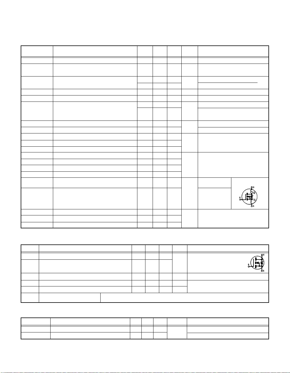
Modified MOSFET
ing the internal inductances.
symbol show-
C
iss
C
oss
C
rss
Input Capacitance — 7400 — VGS = 0V, VDS = -25 V
Output Capacitance — 3200 — p F f = 1.0MHz
Reverse Transfer Capacitance — 540 —
Source-Drain Diode Ratings and Characteristics
Parameter Min Typ Max Units Test Conditions
I
Continuous Source Current (Body Diode) — — -48
S
I
Pulse Source Current (Body Diode) — — -192
SM
V
Diode Forward Voltage — — -3.0 V Tj = 25°C, IS = -48A, VGS = 0V
SD
t
Reverse Recovery Time — — 48 0 ns Tj = 25°C, IF = -48A, di/dt ≤ -100A/µs
rr
Q
Reverse Recovery Charge — — 3.7 µCV
RR
t
Forward Tur n-On Time
on
Intrinsic turn-on time is negligible. Turn-on speed is substantially controlled by LS + LD.
Thermal Resistance
Parameter Min Typ Max Units Test Conditions
R
thJC
R
thJ-PCB
* Limited by Pin diameter
Junction-to-Case — — 0.42
Junction-to-PC board — TBD — K/W Soldered to a copper-clad PC board
Modified MOSFET symbol
A
showing the integral reverse
p-n junction rectifier.
≤ -50V
DD
 Loading...