

International Rectifier IRH9230 Datasheet
Provisional Data Sheet No. PD-9.1391
Next Data SheetIndex
Previous Datasheet
To Order
AVALANCHE ENERGY AND dv/dt RATED
HEXFET
-200 Volt, 0.8
International Rectifier’s P-Channel RAD HARD technology
HEXFETs demonstrate excellent threshold v oltage stability
and breakdown voltage stability at total radiation doses as
high as 105 Rads (Si). Under identical pre- and post-radiation
test conditions, International Rectifier’s P-Channel RAD
HARD HEXFETs retain identical electrical specifications up
to 1 x 10⁵ Rads (Si) total dose. No compensation in gate
drive circuitry is required. These de vices are also capable of
surviving transient ionization pulses as high as 1 x 10¹² Rads
(Si)/Sec, and return to normal operation within a few
microseconds. Single Event Effect (SEE) testing of
International Rectifier P-Channel RAD HARD HEXFETs has
demonstrated virtual immunity to SEE failure. Since the PChannel RAD HARD process utilizes International Rectifier’s
patented HEXFET technology, the user can expect the
highest quality and reliability in the industry.
P-Channel RAD HARD HEXFET transistors also feature all
of the well-established advantages of MOSFETs, such as
voltage control,very fast switching, ease of paralleling and
temperature stability of the electrical parameters.
They are well-suited for applications such as switching power
supplies, motor controls, inverters, choppers, audio amplifiers
and high-energy pulse circuits in space and weapons
environments.
®
TRANSISTOR
ΩΩ
Ω, RAD HARD HEXFET
ΩΩ
IRH9230
P-CHANNEL
RAD HARD
Product Summary
Part Number BV
DSS
IRH9230 -200V 0.8Ω -6.5A
Features:
n Radiation Hardened up to 1 x 10
n Single Event Burnout (SEB) Hardened
n Single Event Gate Rupture (SEGR) Hardened
n Gamma Dot (Flash X-Ray) Hardened
n Neutron Tolerant
n Identical Pre- and Post-Electrical Test Conditions
n Repetitive Avalanche Rating
n Dynamic dv/dt Rating
n Simple Drive Requirements
n Ease of Paralleling
n Hermetically Sealed
R
DS(on)
5
Rads (Si)
I
D
Absolute Maximum Ratings
Parameter IRH9230 Units
ID @ VGS = -12V , TC = 25°C Continuous Drain Current -6.5
ID @ VGS = -12V, TC = 100°C Continuous Drain Current -4.1
I
DM
PD @ TC = 25°C Max. Power Dissipation 75 W
V
GS
E
AS
I
AR
E
AR
dv/dt Peak Diode Recovery dv/dt -5.0
T
J
T
STG
Notes: See page 4
Pulsed Drain Current -26
Linear Derating Factor 0.2 W/K
Gate-to-Source V oltage ±20 V
Single Pulse Avalanche Energy 330 mJ
Avalanche Current -6.5 A
Repetitive Avalanche Energy 7.5 mJ
Operating Junction -55 to 150
Storage T emperature Range
Lead T emperature 300 (0.063 in. (1 .6mm) from case for 10s)
Weight 11.5 (typical) g
Pre-Radiation
A
V/ns
o
C
IRH9230 Device Pre-Radiation
Next Data SheetIndex
Previous Datasheet
To Order
Electrical Characteristics @ Tj = 25°C (Unless Otherwise Specified)
Parameter Min. Typ. Max. Units Test Conditions
BV
DSS
∆BV
R
DS(on)
V
GS(th)
g
fs
I
DSS
I
GSS
I
GSS
Q
g
Q
gs
Q
gd
t
d(on)
t
r
t
d(off)
t
f
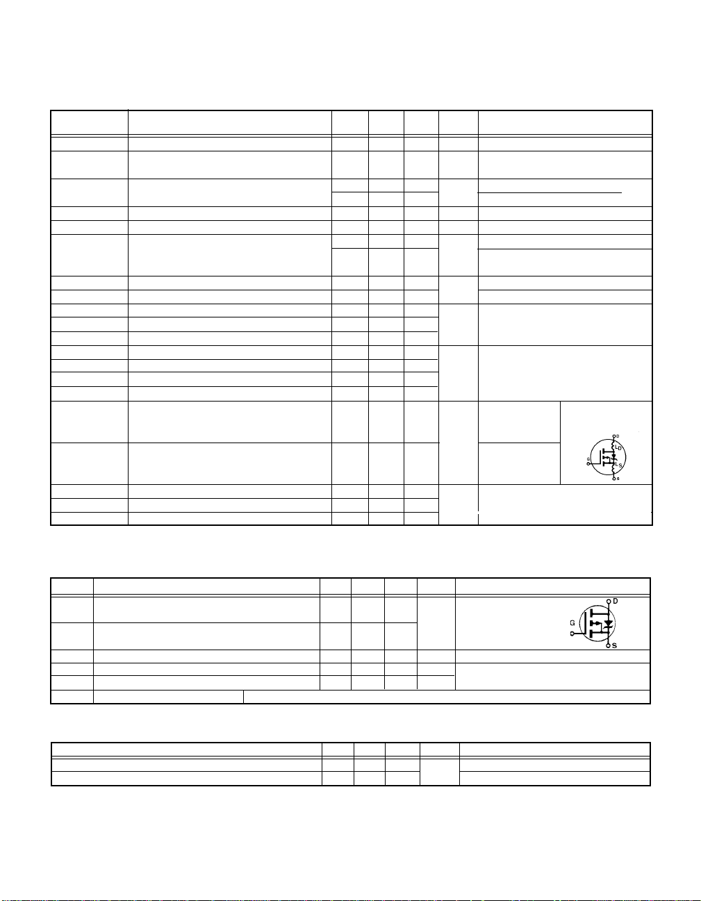
L
D
L
S
C
iss
C
oss
C
rss
DSS
Drain-to-Source Breakdown V oltage -200 — — V VGS = 0V, ID = 1.0 mA
/∆TJT emperature Coefficient of Breakdo wn — -0.10 — V/°C Reference to 25°C, ID = -1.0 mA
V oltage
Static Drain-to-Source — — 0.8 VGS = -12V, ID = -4.1A
On-State Resistance — — 0.92 Ω VGS = -12V, ID = -6.5A
Gate Threshold V oltage -2.0 — -4.0 V VDS = VGS, ID = -1.0 mA
Forw ard Tr ansconductance 2.5 — — S ( )VDS > -15V, IDS = -6.5A
Zero Gate Voltage Drain Current — — -25 VDS = 0.8 x Max. Rating,VGS = 0V
— — -250 VDS = 0.8 x Max. Rating
Gate-to-Source Leakage Forward — — -100 VGS = -20V
Gate-to-Source Leakage Reverse — — 100 VGS = +20V
T otal Gate Charge — — 3 5 VGS = -12V, ID = -6.5A
Gate-to-Source Charge — — 10 VDS = Max. Rating x 0.5
Gate-to-Drain (“Miller”) Charge — — 25
T urn-On Delay Time — — 50 VDD = -50V, ID = -6.5A, RG = 7.5Ω
Rise Time — — 9 0
T urn-Off Delay Time — — 9 0
Fall Time — — 9 0
Internal Drain Inductance — 5.0 —
Internal Source Inductance — 15 —
Input Capacitance — 900 — VGS = 0V, VDS = -25V
Output Capacitance — 250 — f = 1.0 MHz
Reverse Transfer Capacitance — 45 —
Ω
µA
nA
nC
ns
Measured from the
drain lead, 6mm (0.25
in.) from package to
center of die.
nH
Measured from the
source lead, 6mm
(0.25 in.) from package
to source bonding pad.
pF
VGS = 0V, TJ = 125°C
Modified MOSFET
symbol showing the
internal inductances.
Source-Drain Diode Ratings and Characteristics
Parameter Min. Typ. Max. Units Test Conditions
I
Continuous Source Current — — -6.5 Modified MOSFET symbol
S
(Body Diode)
I
Pulse Source Current — — -26
SM
(Body Diode)
V
Diode Forward Voltage — — -5.0 V Tj = 25°C, IS = -6.5A, VGS = 0V
SD
t
Reverse Recovery Time — — 400 ns Tj = 25°C, IF = -6.5A, di/dt ≤ -100 A/µs
rr
Q
Reverse Recovery Charge — — 4.0 µCV
RR
t
Forward T urn-On Time Intrinsic turn-on time is negligible. Turn-on speed is substantially controlled by L
on
Thermal Resistance
Parameter Min. Typ. Max. Units Test Conditions
R
R
thJC
thJA
Junction-to-Case — — 1.67
Junction-to-Ambient — 30 —
Notes: See page 4
showing the integral Reverse
p-n junction rectifier.
A
K/W
≤ -14V
DD
+ LD.
S
 Loading...