

International Rectifier IRGPH50S Datasheet
Preliminary Data SheetPD - 9.760
Index
Previous Datasheet
Next Data Sheet
To Order
IRGPH50S
INSULATED GATE BIPOLAR TRANSISTOR
Features
• Switching-loss rating includes all "tail" losses
• Optimized for line frequency operation (to 400Hz)
See Fig. 1 for Current vs. Frequency curve
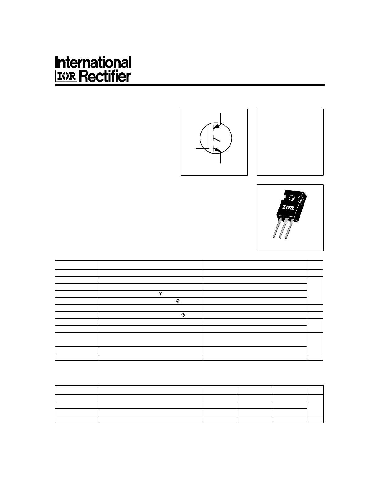
G
C
E
Standard Speed IGBT
V
= 1200V
CES
V
@VGE = 15V, IC = 33A
CE(sat)
≤ 2.0V
n-channel
Description
Insulated Gate Bipolar Transistors (IGBTs) from International Rectifier have
higher usable current densities than comparable bipolar transistors, while at
the same time having simpler gate-drive requirements of the familiar power
MOSFET. They provide substantial benefits to a host of high-voltage, highcurrent applications.
TO-247AC
Absolute Maximum Ratings
Parameter Max. Units
V
CES
IC @ TC = 25°C Continuous Collector Current 57
IC @ TC = 100°C Continuous Collector Current 33 A
I
CM
I
LM
V
GE
E
ARV
PD @ TC = 25°C Maximum Power Dissipation 200 W
PD @ TC = 100°C Maximum Power Dissipation 78
T
J
T
STG
Collector-to-Emitter Voltage 1200 V
Pulsed Collector Current 110
Clamped Inductive Load Current 110
Gate-to-Emitter Voltage ±20 V
Reverse Voltage Avalanche Energy 20 mJ
Operating Junction and -55 to +150
Storage Temperature Range °C
Soldering Temperature, for 10 sec. 300 (0.063 in. (1.6mm) from case)
Mounting torque, 6-32 or M3 screw. 10 lbf•in (1.1N•m)
Thermal Resistance
R
θJC
R
θCS
R
θJA
Wt Weight — 6 (0.21) — g (oz)
Parameter Min. Typ. Max. Units
Junction-to-Case — — 0.64
Case-to-Sink, flat, greased surface — 0.24 — °C/W
Junction-to-Ambient, typical socket mount — — 40
Revision 0
C-49
IRGPH50S
Index
Previous Datasheet
Next Data Sheet
To Order
Electrical Characteristics @ TJ = 25°C (unless otherwise specified)
Parameter Min. Typ. Max. Units Conditions
V
(BR)CES
V
(BR)ECS
∆V
(BR)CES
V
CE(on)
V
GE(th)
∆V
GE(th)
g
fe
I
CES
I
GES
Switching Characteristics @ TJ = 25°C (unless otherwise specified)
Parameter Min. Typ. Max. Units Conditions
Q
g
Q
ge
Q
gc
t
d(on)
t
r
t
d(off)
t
f
E
on
E
off
E
ts
t
d(on)
t
r
t
d(off)
t
f
E
ts
L
E
C
ies
C
oes
C
res
Notes:
Repetitive rating; VGE=20V, pulse width
limited by max. junction temperature.
( See fig. 13b )
VCC=80%(V
RG= 5.0Ω, ( See fig. 13a )
Collector-to-Emitter Breakdown Voltage 1200 — — V VGE = 0V, IC = 250µA
Emitter-to-Collector Breakdown Voltage 20 — — V VGE = 0V, IC = 1.0A
/∆T
Temperature Coeff. of Breakdown Voltage — 1.3 — V/°C VGE = 0V, IC = 1.0mA
J
Collector-to-Emitter Saturation Voltage — 1.7 2.0 IC = 33A VGE = 15V
— 2.2 — V IC = 57A See Fig. 2, 5
— 2.0 — IC = 33A, TJ = 150°C
Gate Threshold Voltage 3.0 — 5.5 VCE = VGE, IC = 250µA
/∆TJTemperature Coeff. of Threshold Voltage — -13 — mV/°C VCE = VGE, IC = 250µA
Forward Transconductance — 19 — S VCE = 100V, IC = 33A
Zero Gate Voltage Collector Current — — 250 µA VGE = 0V, VCE = 1200V
— — 1000 VGE = 0V, VCE = 1200V, TJ = 150°C
Gate-to-Emitter Leakage Current — — ±100 nA VGE = ±20V
Total Gate Charge (turn-on) — 72 108 IC = 33A
Gate - Emitter Charge (turn-on) — 16 24 nC VCC = 400V See Fig. 8
Gate - Collector Charge (turn-on) — 19 30 VGE = 15V
Turn-On Delay Time — 62 — TJ = 25°C
Rise Time — 77 — ns IC = 33A, VCC = 960V
Turn-Off Delay Time — 1200 1800 VGE = 15V, RG = 5.0Ω
Fall Time — 780 1200 Energy losses include "tail"
Turn-On Switching Loss — 3.0 —
Turn-Off Switching Loss — 26 — mJ See Fig. 9, 10, 11, 14
Total Switching Loss — 29 44
Turn-On Delay Time — 52 — TJ = 150°C,
Rise Time — 76 — ns IC = 33A, VCC = 960V
Turn-Off Delay Time — 1300 — VGE = 15V, RG = 5.0Ω
Fall Time — 2100 — Energy losses include "tail"
Total Switching Loss — 55 — mJ See Fig. 10, 14
Internal Emitter Inductance — 13 — nH Measured 5mm from package
Input Capacitance — 1900 — VGE = 0V
Output Capacitance — 140 — pF VCC = 30V See Fig. 7
Reverse Transfer Capacitance — 24 — ƒ = 1.0MHz
Pulse width 5.0µs,
single shot.
), VGE=20V, L=10µH,
CES
Repetitive rating; pulse width limited
by maximum junction temperature.
Pulse width ≤ 80µs; duty factor ≤ 0.1%.
Refer to Section D - page D-13
Package Outline 3 - JEDEC Outline TO-247AC (TO-3P)
C-50
 Loading...