

International Rectifier IRGPH50MD2 Datasheet

PD - 9.1047A
Next Data SheetIndex
Previous Datasheet
To Order
IRGPH50MD2
INSULATED GATE BIPOLAR TRANSISTOR
WITH ULTRAFAST SOFT RECOVERY
Short Circuit Rated
Fast CoPack IGBT
DIODE
Features
• Short circuit rated -10µs @125°C, V
• Switching-loss rating includes all "tail" losses
• HEXFREDTM soft ultrafast diodes
• Optimized for medium operating frequency ( 1 to
10kHz) See Fig. 1 for Current vs. Frequency curve
GE
= 15V
G
C
V
= 1200V
CES
V
CE(sat)
≤ 2.9V
@VGE = 15V, IC = 23A
E
n-channel
Description
Co-packaged IGBTs are a natural extension of International Rectifier's well
known IGBT line. They provide the convenience of an IGBT and an ultrafast
recovery diode in one package, resulting in substantial benefits to a host of
high-voltage, high-current, applications.
These new short circuit rated devices are especially suited for motor control
and other applications requiring short circuit withstand capability.
TO-247AC
Absolute Maximum Ratings
Parameter Max. Units
V
CES
IC @ TC = 25°C Continuous Collector Current 42
IC @ TC = 100°C Continuous Collector Current 23
I
CM
I
LM
IF @ TC = 100°C Diode Continuous Forward Current 16
I
FM
t
sc
V
GE
PD @ TC = 25°C Maximum Power Dissipation 200 W
PD @ TC = 100°C Maximum Power Dissipation 78
T
J
T
STG
Collector-to-Emitter Voltage 1200 V
Pulsed Collector Current 84 A
Clamped Inductive Load Current 84
Diode Maximum Forward Current 84
Short Circuit Withstand Time 10 µs
Gate-to-Emitter Voltage ± 20 V
Operating Junction and -55 to +150
Storage Temperature Range °C
Soldering Temperature, for 10 sec. 300 (0.063 in. (1.6mm) from case)
Mounting torque, 6-32 or M3 screw. 10 lbf•in (1.1 N•m)
Thermal Resistance
R
θJC
R
θJC
R
θCS
R
θJA
Wt Weight — 6 (0.21) — g (oz)
Parameter Min. Typ. Max. Units
Junction-to-Case - IGBT — — 0.64
Junction-to-Case - Diode — — 0.83 °C/W
Case-to-Sink, flat, greased surface — 0.24 —
Junction-to-Ambient, typical socket mount — — 40
C-481
Revision 1

IRGPH50MD2
Next Data SheetIndex
Previous Datasheet
To Order
Electrical Characteristics @ TJ = 25°C (unless otherwise specified)
Parameter Min. Typ. Max. Units Conditions
V
(BR)CES
∆V
(BR)CES
V
CE(on)
V
GE(th)
∆V
GE(th)
g
fe
I
CES
V
FM
I
GES
Switching Characteristics @ TJ = 25°C (unless otherwise specified)
Parameter Min. Typ. Max. Units Conditions
Q
g
Q
ge
Q
gc
t
d(on)
t
r
t
d(off)
t
f
E
on
E
off
E
ts
t
sc
t
d(on)
t
r
t
d(off)
t
f
E
ts
L
E
C
ies
C
oes
C
res
t
rr
I
rr
Q
rr
di
(rec)M
Notes:
Repetitive rating; VGE=20V, pulse width limited
by max. junction temperature. ( See fig. 20 )
Collector-to-Emitter Breakdown Voltage 1200 — — V VGE = 0V, IC = 250µA
/∆T
Temperature Coeff. of Breakdown Voltage — 1.1 — V/°C VGE = 0V , IC = 1.0mA
J
Collector-to-Emitter Saturation Voltage — 2.3 2.9 IC = 23A VGE = 15V
— 3.0 — V IC = 42A See Fig. 2, 5
— 2.8 — IC = 23A, TJ = 150°C
Gate Threshold Voltage 3.0 — 5.5 VCE = VGE, IC = 250µA
/∆TJTemperature Coeff. of Threshold Voltage — -13 — mV/°C VCE = VGE, IC = 250µA
Forward Transconductance 11 15 — S VCE = 100V, IC = 23A
Zero Gate Voltage Collector Current — — 250 µA VGE = 0V, VCE = 1200V
— — 6500 VGE = 0V, VCE =1200V, TJ = 150°C
Diode Forward Voltage Drop — 2.5 3.0 V IC = 16A See Fig. 13
— 2.1 2.5 IC = 16A, TJ = 150°C
Gate-to-Emitter Leakage Current — — ±100 nA VGE = ±20V
Total Gate Charge (turn-on) — 89 130 IC = 23A
Gate - Emitter Charge (turn-on) — 22 33 nC VCC = 400V
Gate - Collector Charge (turn-on) — 26 39 See Fig. 8
Turn-On Delay Time — 100 — TJ = 25°C
Rise Time — 140 — ns IC = 23A, VCC = 960V
Turn-Off Delay Time — 510 770 VGE = 15V, RG = 5.0 Ω
Fall Time — 470 730 Energy losses include "tail" and
Turn-On Switching Loss — 3.0 — diode reverse recovery.
Turn-Off Switching Loss — 8.0 — mJ See Fig. 9, 10, 11, 18
Total Switching Loss — 11 17
Short Circuit Withstand Time 10 — — µs VCC = 720V, TJ = 125°C
VGE = 15V, RG = 5.0 Ω
Turn-On Delay Time — 86 — TJ = 150°C, See Fig. 9, 10, 11, 18
Rise Time — 130 — ns IC = 23A, VCC = 960V
Turn-Off Delay Time — 800 — VGE = 15V, RG = 5.0 Ω
Fall Time — 920 — Energy losses include "tail" and
Total Switching Loss — 20 — mJ diode reverse recovery
Internal Emitter Inductance — 13 — nH Measured 5mm from package
Input Capacitance — 1900 — VGE = 0V
Output Capacitance — 140 — pF VCC = 30V See Fig. 7
Reverse Transfer Capacitance — 24 — ƒ = 1.0MHz
Diode Reverse Recovery Time — 90 135 ns TJ = 25°C See Fig.
— 164 245 TJ = 125°C 14 IF = 16A
Diode Peak Reverse Recovery Charge — 5.8 10 A TJ = 25°C See Fig.
— 8.3 15 TJ = 125°C 15 VR = 200V
Diode Reverse Recovery Charge — 260 675 nC TJ = 25°C See Fig.
— 680 1838 TJ = 125°C 16 di/dt = 200A/µs
/dt Diode Peak Rate of Fall of Recovery — 120 — A/µs TJ = 25°C See Fig.
During t
b
— 76 — TJ = 125°C 17
VCC=80%(V
), VGE=20V, L=10µH,
CES
RG= 5.0 Ω, ( See fig. 19 )
Pulse width 5.0µs,
single shot.
Pulse width ≤ 80µs; duty factor ≤ 0.1%.
C-482
IRGPH50MD2
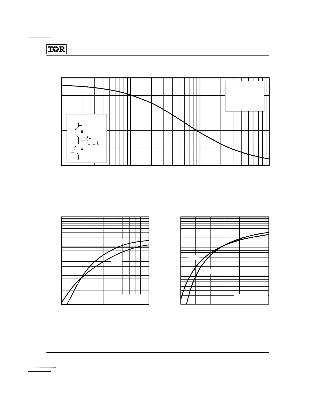
f, Frequency (kHz)
Load Current (A)
CE
C
I , Collector-to-Emitter Current (A)
, Collector-to-Em
er Voltage (V)
C
I , Collector-to-Emitter Cu rrent (A)
, Gate-to-Em
er Voltage (V)
GE
To Order
Next Data SheetIndex
Previous Datasheet
25
Duty c ycle: 50 %
T = 125°C
J
T = 90 °C
20
15
60% of rated
voltage
10
5
0
0.1 1 10 100
Fig. 1 - Typical Load Current vs. Frequency
(Load Current = I
of fundamental)
RMS
sink
Gate drive as spe cified
Turn-on l osses include
effects of rev erse reco very
Power Dissi p ation = 40W
100 0
100
10
1
1 10
V
25°C
150°C
V = 15V
GE
20µs PULSE WIDTH
itt
Fig. 2 - Typical Output Characteristics
C-483
100 0
100
150°C
10
1
5 10 15 20
25°C
V = 1 0 0V
C C
5µs PUL S E W IDTH
V
itt
Fig. 3 - Typical Transfer Characteristics
 Loading...