

International Rectifier IRGP430UD2 Datasheet
PD - 9.1063
Next Data SheetIndex
Previous Datasheet
To Order
IRGP430UD2
INSULATED GATE BIPOLAR TRANSISTOR
UltraFast CoPack IGBT
WITH ULTRAFAST SOFT RECOVERY DIODE
Features
• Switching-loss rating includes all "tail" losses
• HEXFREDTM soft ultrafast diodes
• Optimized for high operating frequency (over 5kHz)
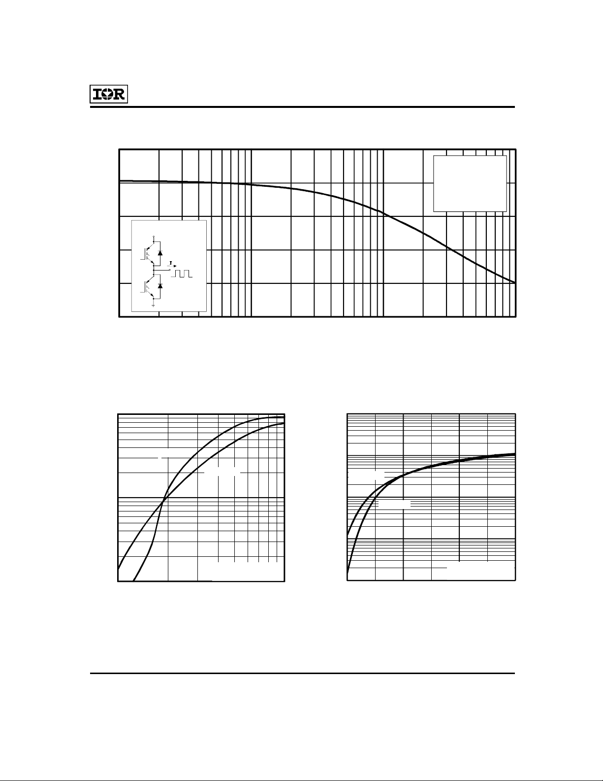
See Fig. 1 for Current vs. Frequency curve
G
C
V
= 500V
CES
V
CE(sat)
≤ 3.0V
@VGE = 15V, IC = 15A
E
n-channel
Description
Co-packaged IGBTs are a natural extension of International Rectifier's well
known IGBT line. They provide the convenience of an IGBT and an ultrafast
recovery diode in one package, resulting in substantial benefits to a host of
high-voltage, high-current, motor control, UPS and power supply applications.
O-247AC
T
Absolute Maximum Ratings
Parameter Max. Units
V
CES
IC @ TC = 25°C Continuous Collector Current 25
IC @ TC = 100°C Continuous Collector Current 15
I
CM
I
LM
IF @ TC = 100°C Diode Continuous Forward Current 12
I
FM
V
GE
PD @ TC = 25°C Maximum Power Dissipation 100 W
PD @ TC = 100°C Maximum Power Dissipation 42
T
J
T
STG
Collector-to-Emitter Voltage 500 V
Pulsed Collector Current 50 A
Clamped Inductive Load Current 50
Diode Maximum Forward Current 50
Gate-to-Emitter Voltage ± 20 V
Operating Junction and -55 to +150
Storage Temperature Range °C
Soldering Temperature, for 10 sec. 300 (0.063 in. (1.6mm) from case)
Mounting Torque, 6-32 or M3 Screw. 10 lbf•in (1.1 N•m)
Thermal Resistance
R
θJC
R
θJC
R
θCS
R
θJA
Wt Weight — 6 (0.21) — g (oz)
Parameter Min. Typ. Max. Units
Junction-to-Case - IGBT — — 1.2
Junction-to-Case - Diode — — 2.5 °C/W
Case-to-Sink, flat, greased surface — 0.24 —
Junction-to-Ambient, typical socket mount — — 40
C-633
Revision 1
IRGP430UD2
Next Data SheetIndex
Previous Datasheet
To Order
Electrical Characteristics @ TJ = 25°C (unless otherwise specified)
Parameter Min. Typ. Max. Units Conditions
V
(BR)CES
∆V
(BR)CES
V
CE(on)
V
GE(th)
∆V
GE(th)
g
fe
I
CES
V
FM
I
GES
Switching Characteristics @ TJ = 25°C (unless otherwise specified)
Parameter Min. Typ. Max. Units Conditions
Q
g
Q
ge
Q
gc
t
d(on)
t
r
t
d(off)
t
f
E
on
E
off
E
ts
t
d(on)
t
r
t
d(off)
t
f
E
ts
L
E
C
ies
C
oes
C
res
t
rr
I
rr
Q
rr
di
(rec)M
Notes:
Repetitive rating; VGE=20V, pulse width
limited by max. junction temperature.
( See fig. 20 )
Collector-to-Emitter Breakdown Voltage 500 — — V VGE = 0V, IC = 250µA
/∆T
Temp. Coeff. of Breakdown Voltage — 0.46 — V/°C VGE = 0V, IC = 1.0mA
J
Collector-to-Emitter Saturation Voltage — 2.3 3.0 IC = 15A VGE = 15V
— 2.8 — V IC = 25A See Fig. 2, 5
— 2.6 — IC = 15A, TJ = 150°C
Gate Threshold Voltage 3.0 — 5.5 VCE = VGE, IC = 250µA
/∆TJTemp. Coeff. of Threshold Voltage — -11 — mV/°C VCE = VGE, IC = 250µA
Forward Transconductance 2.3 8.1 — S VCE = 100V, IC = 15A
Zero Gate Voltage Collector Current — — 250 µA VGE = 0V, VCE = 500V
— — 2500 VGE = 0V, VCE = 500V, TJ = 150°C
Diode Forward Voltage Drop — 1.4 1.7 V IC = 12A See Fig. 13
— 1.3 1.6 IC = 12A, TJ = 150°C
Gate-to-Emitter Leakage Current — — ±100 nA VGE = ±20V
Total Gate Charge (turn-on) — 31 47 IC = 15A
Gate - Emitter Charge (turn-on) — 6.2 9.2 nC VCC = 400V
Gate - Collector Charge (turn-on) — 12 19 See Fig. 8
Turn-On Delay Time — 73 — TJ = 25°C
Rise Time — 72 — ns IC = 15A, VCC = 400V
Turn-Off Delay Time — 120 180 VGE = 15V, RG = 23Ω
Fall Time — 100 150 Energy losses include "tail" and
Turn-On Switching Loss — 0.7 — diode reverse recovery.
Turn-Off Switching Loss — 0.4 — mJ See Fig. 9, 10, 11, 18
Total Switching Loss — 1.1 1.7
Turn-On Delay Time — 77 — TJ = 150°C, See Fig. 9, 10, 11, 18
Rise Time — 75 — ns IC = 15A, VCC = 400V
Turn-Off Delay Time — 200 — VGE = 15V, RG = 23Ω
Fall Time — 190 — Energy losses include "tail" and
Total Switching Loss — 1.5 — mJ diode reverse recovery.
Internal Emitter Inductance — 13 — nH Measured 5mm from package
Input Capacitance — 660 — VGE = 0V
Output Capacitance — 110 — pF VCC = 30V See Fig. 7
Reverse Transfer Capacitance — 12 — ƒ = 1.0MHz
Diode Reverse Recovery Time — 42 60 ns TJ = 25°C See Fig.
— 80 120 TJ = 125°C 14 IF = 12A
Diode Peak Reverse Recovery Current — 3.5 6.0 A TJ = 25°C See Fig.
— 5.6 10 TJ = 125°C 15 VR = 200V
Diode Reverse Recovery Charge — 80 180 nC TJ = 25°C See Fig.
— 220 600 TJ = 125°C 16 di/dt = 200A/µs
/dt Diode Peak Rate of Fall of Recovery — 180 — A/µs TJ = 25°C See Fig.
During t
b
— 116 — TJ = 125°C 17
VCC=80%(V
), VGE=20V, L=10µH,
CES
RG= 23Ω, ( See fig. 19 )
Pulse width 5.0µs,
single shot.
Pulse width ≤ 80µs; duty factor ≤ 0.1%.
C-634
IRGP430UD2
A
CE
C
I , Collector-to-Emitter Current (A)
, Collector-to-Em
er Voltag e (V)
C
I , Collector-to-Em itter Current (A)
,
GE
To Order
Next Data SheetIndex
Previous Datasheet
20
Du ty cycle: 5 0 %
T = 125°C
J
T = 90°C
16
12
60% of r a ted
v olta ge
8
Load Current (A)
4
0
0.1 1 10 100
f, Frequency (kHz)
Fig. 1 - Typical Load Current vs. Frequency
(Load Current = I
of fundamental)
RMS
sink
Ga te dri ve as specifie d
Tu rn-on lo sses incl u de
effects of re verse reco very
Po wer D issipation = 24W
100
T = 25°C
J
T = 150°C
J
10
V = 15V
G E
1
1 10
V
20µs P ULSE WIDTH
itt
Fig. 2 - Typical Output Characteristics
C-635
1000
100
T = 1 50°C
J
10
1
0.1
5 10 15 20
T = 25°C
J
V
Gate-to-Em itter Voltage (V)
V = 100V
CC
5µs PUL SE W IDTH
Fig. 3 - Typical Transfer Characteristics
 Loading...