

International Rectifier IRGBC20S Datasheet

IGBT Designer’s Manual
Next Data SheetIndex
Previous Datasheet
To Order
Data Sheets
The IGBT devices listed in this Designer’s
Manual represent International Rectifier’s
IGBT line as of August, 1994. The data
presented in this manual supersedes all
previous specifications.
C-2
PD - 9.687A
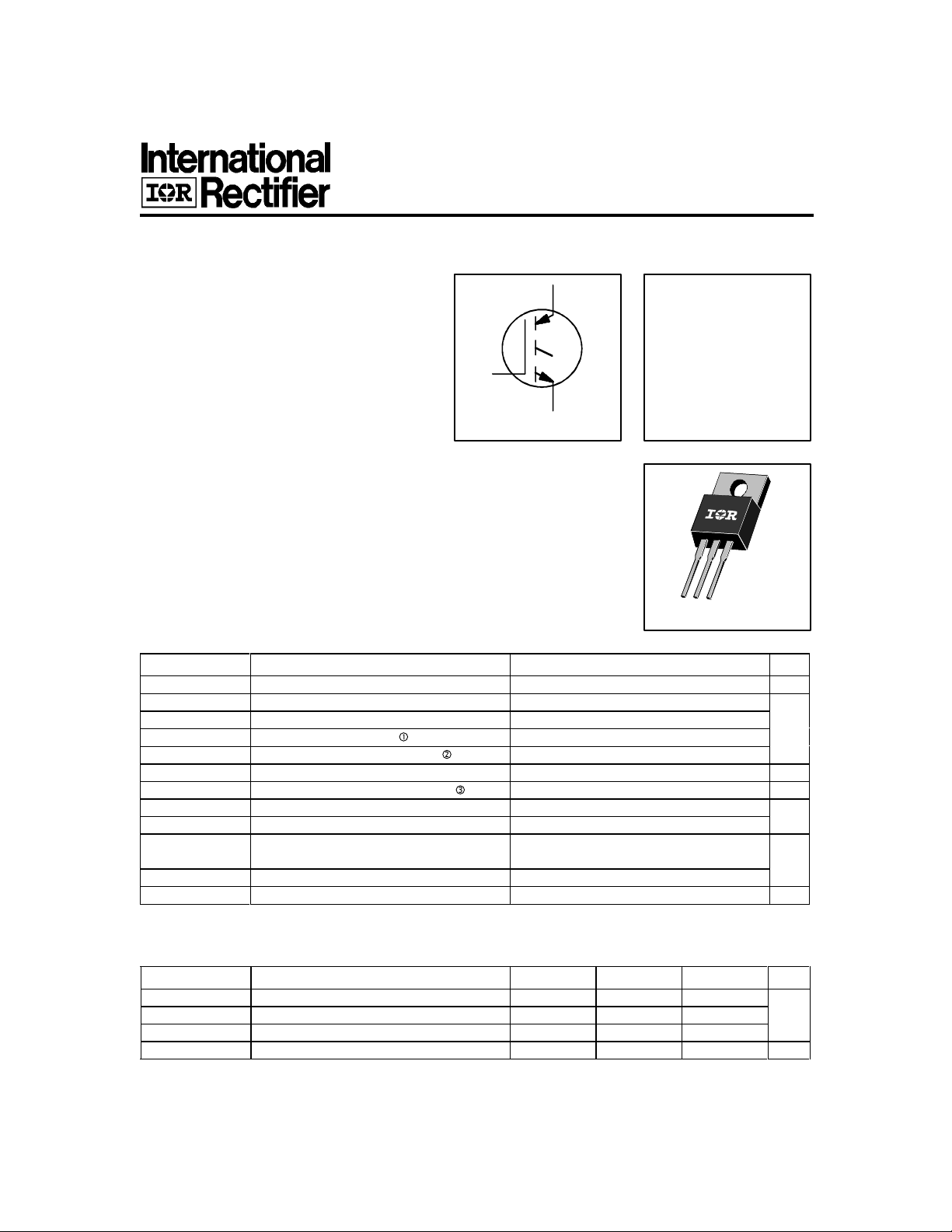
TO-220AB
Next Data SheetIndex
Previous Datasheet
To Order
IRGBC20S
INSULATED GATE BIPOLAR TRANSISTOR
Features
• Switching-loss rating includes all "tail" losses
• Optimized for line frequency operation ( to 400 Hz)
See Fig. 1 for Current vs. Frequency curve
G
C
E
Standard Speed IGBT
V
= 600V
CES
V
@VGE = 15V, IC = 10A
CE(sat)
≤ 2.4V
n-channel
Description
Insulated Gate Bipolar Transistors (IGBTs) from International Rectifier have
higher usable current densities than comparable bipolar transistors, while at
the same time having simpler gate-drive requirements of the familiar power
MOSFET. They provide substantial benefits to a host of high-voltage, highcurrent applications.
Absolute Maximum Ratings
Parameter Max. Units
V
CES
IC @ TC = 25°C Continuous Collector Current 19
IC @ TC = 100°C Continuous Collector Current 10 A
I
CM
I
LM
V
GE
E
ARV
PD @ TC = 25°C Maximum Power Dissipation 60 W
PD @ TC = 100°C Maximum Power Dissipation 24
T
J
T
STG
Collector-to-Emitter Voltage 600 V
Pulsed Collector Current 76
Clamped Inductive Load Current 38
Gate-to-Emitter Voltage ±20 V
Reverse Voltage Avalanche Energy 5.0 mJ
Operating Junction and -55 to +150
Storage Temperature Range °C
Soldering Temperature, for 10 sec. 300 (0.063 in. (1.6mm) from case)
Mounting torque, 6-32 or M3 screw. 10 lbf•in (1.1N•m)
Thermal Resistance
R
θJC
R
θCS
R
θJA
Wt Weight — 2.0 (0.07) — g (oz)
Parameter Min. Typ. Max. Units
Junction-to-Case — — 2.1
Case-to-Sink, flat, greased surface — 0.50 — °C/W
Junction-to-Ambient, typical socket mount — — 80
Revision 0
C-3
IRGBC20S
To Order
Next Data SheetIndex
Previous Datasheet
Electrical Characteristics @ TJ = 25°C (unless otherwise specified)
Parameter Min. Typ. Max. Units Conditions
V
(BR)CES
V
(BR)ECS
∆V
(BR)CES
V
CE(on)
V
GE(th)
∆V
GE(th)
g
fe
I
CES
I
GES
Switching Characteristics @ TJ = 25°C (unless otherwise specified)
Parameter Min. Typ. Max. Units Conditions
Q
g
Q
ge
Q
gc
t
d(on)
t
r
t
d(off)
t
f
E
on
E
off
E
ts
t
d(on)
t
r
t
d(off)
t
f
E
ts
L
E
C
ies
C
oes
C
res
Collector-to-Emitter Breakdown Voltage 600 — — V VGE = 0V, IC = 250µA
Emitter-to-Collector Breakdown Voltage 20 — — V VGE = 0V, IC = 1.0A
/∆T
Temperature Coeff. of Breakdown Voltage — 0.75 — V/°C VGE = 0V, IC = 1.0mA
J
Collector-to-Emitter Saturation Voltage — 1.8 2.4 IC = 10A VGE = 15V
— 2.4 — V IC = 19A See Fig. 2, 5
— 1.9 — IC = 10A, TJ = 150°C
Gate Threshold Voltage 3.0 — 5.5 VCE = VGE, IC = 250µA
/∆TJTemperature Coeff. of Threshold Voltage — -11 — mV/°C VCE = VGE, IC = 250µA
Forward Transconductance 2.0 5.8 — S VCE = 100V, IC = 10A
Zero Gate Voltage Collector Current — — 250 µA VGE = 0V, VCE = 600V
— — 1000 VGE = 0V, VCE = 600V, TJ = 150°C
Gate-to-Emitter Leakage Current — — ±100 nA VGE = ±20V
Total Gate Charge (turn-on) — 16 26 IC = 10A
Gate - Emitter Charge (turn-on) — 2.3 4.0 nC VCC = 400V See Fig. 8
Gate - Collector Charge (turn-on) — 7.0 12 VGE = 15V
Turn-On Delay Time — 24 — TJ = 25°C
Rise Time — 23 — ns IC = 10A, VCC = 480V
Turn-Off Delay Time — 820 1200 VGE = 15V, RG = 50Ω
Fall Time — 910 1600 Energy losses include "tail"
Turn-On Switching Loss — 0.24 —
Turn-Off Switching Loss — 3.9 — mJ See Fig. 9, 10, 11, 14
Total Switching Loss — 4.1 6.0
Turn-On Delay Time — 26 — TJ = 150°C,
Rise Time — 30 — ns IC = 10A, VCC = 480V
Turn-Off Delay Time — 1100 — VGE = 15V, RG = 50Ω
Fall Time — 1800 — Energy losses include "tail"
Total Switching Loss — 7.0 — mJ See Fig. 10, 14
Internal Emitter Inductance — 7.5 — nH Measured 5mm from package
Input Capacitance — 360 — VGE = 0V
Output Capacitance — 36 — pF VCC = 30V See Fig. 7
Reverse Transfer Capacitance — 5.2 — ƒ = 1.0MHz
Notes:
Repetitive rating; VGE=20V, pulse width
limited by max. junction temperature.
( See fig. 13b )
VCC=80%(V
RG= 50Ω, ( See fig. 13a )
), VGE=20V, L=10µH,
CES
Repetitive rating; pulse width limited
by maximum junction temperature.
Pulse width ≤ 80µs; duty factor ≤ 0.1%.
C-4
Pulse width 5.0µs,
single shot.
 Loading...