

International Rectifier IRG4RC10KD Datasheet
PD 91736A
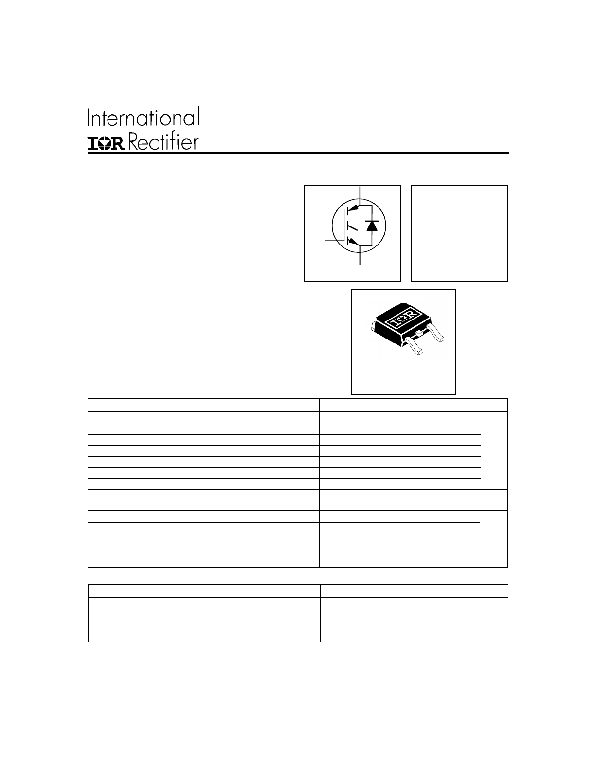
IRG4RC10KD
INSULATED GATE BIPOLAR TRANSISTOR WITH
ULTRAFAST SOFT RECOVERY DIODE
Features
• Short Circuit Rated UltraFast: Optimized for
high operating frequencies >5.0 kHz , and Short
Circuit Rated to 10µs @ 125°C, V
• Generation 4 IGBT design provides tighter
parameter distribution and higher efficiency than
GE
= 15V
G
previous generation
TM
• IGBT co-packaged with HEXFRED
ultra-soft-recovery anti-parallel diodes for use in
ultrafast,
n-channel
bridge configurations
• Industry standard TO-252AA package
Benefits
• Latest generation 4 IGBT's offer highest power density
motor controls possible
• HEXFRED
TM
diodes optimized for performance with IGBTs.
Minimized recovery characteristics reduce noise, EMI and
switching losses
• For hints see design tip 97003
Absolute Maximum Ratings
Parameter Max. Units
V
CES
IC @ TC = 25°C Continuous Collector Current 9.0
IC @ TC = 100°C Continuous Collector Current 5.0
I
CM
I
LM
IF @ TC = 100°C Diode Continuous Forward Current 4.0
I
FM
t
sc
V
GE
PD @ TC = 25°C Maximum Power Dissipation 38
PD @ TC = 100°C Maximum Power Dissipation 15
T
J
T
STG
Collector-to-Emitter Voltage 600 V
Pulsed Collector CurrentQ 18 A
Clamped Inductive Load Current R 18
Diode Maximum Forward Current 16
Short Circuit Withstand Time 10 µ s
Gate-to-Emitter Voltage ± 20 V
Operating Junction and -55 to +150
Storage Temperature Range °C
Soldering Temperature, for 10 sec. 300 (0.063 in. (1.6mm) from case)
C
E
D-PAK
TO-252AA
Short Circuit Rated
UltraFast IGBT
V
= 600V
CES
V
CE(on) typ.
@VGE = 15V, IC = 5.0A
= 2.39V
W
Thermal Resistance
Parameter Typ. Max. Units
R
θJC
R
θJC
R
θJA
Wt Weight 0.3 (0.01) ––– g (oz)
* When mounted on 1" square PCB (FR-4 or G-10 Material).
For recommended footprint and soldering techniques refer to application note #AN-994
Junction-to-Case - IGBT ––– 3.3
Junction-to-Case - Diode ––– 7.0
Junction-to-Ambient (PCB mount)* ––– 50
°C/W
www.irf.com 1
12/30/00
IRG4RC10KD
Electrical Characteristics @ T
= 25°C (unless otherwise specified)
J
Parameter Min. Typ. Max. Units Conditions
V
(BR)CES
∆V
(BR)CES
V
CE(on)
Collector-to-Emitter Breakdown Voltageƒ 600 —— VVGE = 0V, IC = 250µA
/∆T
Temperature Coeff. of Breakdown Voltage — 0.58 — V/°CVGE = 0V, IC = 1.0mA
J
Collector-to-Emitter Saturation Voltage — 2.39 2.62 IC = 5.0A VGE = 15V
— 3.25 — VIC = 9.0A See Fig. 2, 5
— 2.63 — IC = 5.0A, TJ = 150°C
V
∆V
g
I
CES
GE(th)
GE(th)
fe
Gate Threshold Voltage 3.0 — 6.5 VCE = VGE, IC = 250µA
/∆TJTemperature Coeff. of Threshold Voltage — -11 — mV/°CVCE = VGE, IC = 250µA
Forward Transconductance „ 1.2 1.8 — SVCE = 50V, IC = 5.0A
Zero Gate Voltage Collector Current ——250 µA VGE = 0V, VCE = 600V
——1000 VGE = 0V, VCE = 600V, TJ = 150°C
V
FM
Diode Forward Voltage Drop — 1.5 1.8 V IC = 4.0A See Fig. 13
— 1.4 1.7 IC = 4.0A, TJ = 150°C
I
GES
Gate-to-Emitter Leakage Current ——±100 nA VGE = ±20V
Switching Characteristics @ TJ = 25°C (unless otherwise specified)
Parameter Min. Typ. Max. Units Conditions
Q
Q
Q
t
d(on)
t
r
t
d(off)
t
f
E
E
E
t
sc
t
d(on)
t
r
t
d(off)
t
f
E
L
C
C
C
t
rr
g
ge
gc
on
off
ts
ts
E
ies
oes
res
Total Gate Charge (turn-on) — 19 29 IC = 5.0A
Gate - Emitter Charge (turn-on) — 2.9 4.3 nC VCC = 400V See Fig.8
Gate - Collector Charge (turn-on) — 9.8 15 VGE = 15V
Turn-On Delay Time — 49 —
Rise Time — 28 — TJ = 25°C
Turn-Off Delay Time — 97 150 IC = 5.0A, VCC = 480V
ns
Fall Time — 140 210 VGE = 15V, RG = 100Ω
Turn-On Switching Loss — 0.25 — Energy losses include "tail"
Turn-Off Switching Loss — 0.14 — mJ and diode reverse recovery
Total Switching Loss — 0.39 0.48 See Fig. 9,10,14
Short Circuit Withstand Time 10 —— µs VCC = 360V, TJ = 125°C
VGE = 15V, RG = 100Ω , V
CPK
< 500V
Turn-On Delay Time — 46 — TJ = 150°C, See Fig. 10,11,14
Rise Time — 32 — IC = 5.0A, VCC = 480V
Turn-Off Delay Time — 100 — VGE = 15V, RG = 100Ω
ns
Fall Time — 310 — Energy losses include "tail"
Total Switching Loss — 0.56 — mJ and diode reverse recovery
Internal Emitter Inductance — 7.5 — nH Measured 5mm from package
Input Capacitance — 220 — VGE = 0V
Output Capacitance — 29 — pF VCC = 30V See Fig. 7
Reverse Transfer Capacitance — 7.5 —ƒ = 1.0MHz
Diode Reverse Recovery Time — 28 42 ns TJ = 25°C See Fig.
— 38 57 TJ = 125°C 14 IF = 4.0A
I
rr
Diode Peak Reverse Recovery Current — 2.9 5.2 A TJ = 25°C See Fig.
— 3.7 6.7 TJ = 125°C 15 VR = 200V
Q
rr
Diode Reverse Recovery Charge — 40 60 nC TJ = 25°C See Fig.
— 70 105 TJ = 125°C 16 di/dt = 200A/µs
di
/dt Diode Peak Rate of Fall of Recovery — 280 — A/µs TJ = 25°C See Fig.
(rec)M
During t
b
— 235 — TJ = 125°C 17
2 www.irf.com
IRG4RC10KD
1.6
For both:
Duty cycle: 50%
T = 125°C
J
T = 9 0°C
1.2
Square wave:
0.8
LOAD CURRENT (A)
0.4
0.0
0.1 1 10 100
60 % o f r a ted
v o l tage
I
Ideal diodes
f, Frequency (KHz)
Fig. 1 - Typical Load Current vs. Frequency
(Load Current = I
of fundamental)
RMS
55
sink
Gate drive as specified
Pow e r D issip ation = W
1.4
100
°
T = 25 C
J
10
C
I , Collector Current (A)
1
1.0 2.0 3.0 4.0 5.0 6.0 7.0
V , Collector-to-Emitter Voltage (V)
CE
T = 150 C
V = 15V
20µs PULSE WIDTH
°
J
GE
Fig. 2 - Typical Output Characteristics
100
10
T = 150 C
C
I , Collector-to-Emitter Current (A)
1
5 10 15 20
°
J
°
T = 25 C
J
V , Gate-to-Emitter Voltage (V)
GE
V = 50V
CC
5µs PULSE WIDTH
Fig. 3 - Typical Transfer Characteristics
www.irf.com 3
 Loading...