

International Rectifier IRG4PSC71UD Datasheet
PD - 91682A
IRG4PSC71UD
INSULATED GATE BIPOLAR TRANSISTOR WITH
UltraFast CoPack IGBT
ULTRAFAST SOFT RECOVERY DIODE
Features
• Generation 4 IGBT design provides tighter
parameter distribution and higher efficiency
(minimum switching and conduction losses) than
prior generations
• IGBT co-packaged with HEXFRED ultrafast, ultrasoft
recovery anti-parallel diodes for use in bridge
configurations
• Industry-benchmark Super-247 package with
higher power handling capability compared to
same footprint TO-247
• Creepage distance increased to 5.35mm
G
n-channel
Benefits
• Generation 4 IGBT's offer highest efficiencies
available
• Maximum power density, twice the power
handling of TO-247, less space than TO-264
• IGBTs optimized for specific application conditions
• HEXFRED diodes optimized for performance with IGBTs
• Cost and space saving in designs that require
multiple, paralleled IGBTs
Absolute Maximum Ratings
Parameter Max. Units
V
CES
IC @ TC = 25°C Continuous Collector Current 85
IC @ TC = 100°C Continuous Collector Current 60
I
CM
I
LM
IF @ TC = 100°C Diode Continuous Forward Current 60
I
FM
V
GE
PD @ TC = 25°C Maximum Power Dissipation 350
PD @ TC = 100°C Maximum Power Dissipation 140
T
J
T
STG
Collector-to-Emitter Voltage 600 V
Pulsed Collector Current 200 A
Clamped Inductive Load Current 200
Diode Maximum Forward Current 350
Gate-to-Emitter Voltage ± 20 V
Operating Junction and -55 to +150
Storage Temperature Range °C
Soldering Temperature, for 10 sec. 300 (0.063 in. (1.6mm) from case)
Thermal Resistance\ Mechanical
Parameter Min. Typ. Max. Units
R
θJC
R
θJC
R
θCS
R
θJA
Junction-to-Case - IGBT ––– ––– 0.36
Junction-to-Case - Diode ––– ––– 0.69 °C/W
Case-to-Sink, flat, greased surface ––– 0.24 –––
Junction-to-Ambient, typical socket mount ––– ––– 38
Recommended Clip Force 20.0(2.0) ––– ––– N (kgf)
Weight ––– 6 (0.21) ––– g (oz)
www.irf.com 1
C
E
SUPER - 247
V
= 600V
CES
V
CE(on) typ.
= 1.67V
@VGE = 15V, IC = 60A
W
5/12/99
IRG4PSC71UD
Electrical Characteristics @ T
= 25°C (unless otherwise specified)
J
Parameter Min. Typ. Max. Units Conditions
V
(BR)CES
∆V
(BR)CES
V
CE(on)
V
GE(th)
∆V
GE(th)
g
fe
I
CES
Collector-to-Emitter Breakdown Voltage 600 ––– ––– V VGE = 0V, IC = 250µA
/∆T
Temperature Coeff. of Breakdown Voltage ––– 0.39 ––– V/°C VGE = 0V, IC = 10mA
J
Collector-to-Emitter Saturation Voltage ––– 1.67 2.0 IC = 60A VGE = 15V
––– 1.95 ––– IC = 100A See Fig. 2, 5
––– 1.71 ––– IC = 60A, TJ = 150°C
V
Gate Threshold Voltage 3.0 ––– 6.0 VCE = VGE, IC = 250µA
/∆TJTemperature Coeff. of Threshold Voltage ––– -13 – –– mV/°C VCE = VGE, IC = 1.5mA
Forward Transconductance 47 70 ––– S VCE = 50V, IC = 60A
Zero Gate Voltage Collector Current ––– ––– 500 µA VGE = 0V, VCE = 600V
––– ––– 13 mA VGE = 0V, VCE = 600V, TJ = 150°C
V
I
GES
FM
Diode Forward Voltage Drop ––– 1.4 1.7 IC = 60A See Fig. 13
––– 1.3 ––– IC = 60A, TJ = 150°C
V
Gate-to-Emitter Leakage Current ––– ––– ±100 nA VGE = ±20V
Switching Characteristics @ TJ = 25°C (unless otherwise specified)
Parameter Min. Typ. Max. Units Conditions
Q
g
Total Gate Charge (turn-on) ––– 340 520 IC = 60A
Qge Gate - Emitter Charge (turn-on) ––– 44 66 nC VCC = 400V See Fig. 8
Q
gc
t
d(on)
t
r
t
d(off)
t
f
E
on
E
off
E
ts
t
d(on)
t
r
t
d(off)
t
f
E
ts
L
E
C
ies
C
oes
C
res
t
rr
I
rr
Q
rr
di
(rec)M
During t
Gate - Collector Charge (turn-on) ––– 160 240 VGE = 15V
Turn-On Delay Time ––– 90 ––– TJ = 25°C
Rise Time ––– 94 ––– ns IC = 60A, VCC = 480V
Turn-Off Delay Time ––– 245 368 VGE = 15V, RG = 5.0Ω
Fall Time ––– 110 167 Energy losses include "tail" and
Turn-On Switching Loss ––– 3.26 ––– diode reverse recovery.
Turn-Off Switching Loss ––– 2.27 ––– mJ See Fig. 9, 10, 11, 18
Total Switching Loss ––– 5.53 7.2
Turn-On Delay Time ––– 91 ––– TJ = 150°C, See Fig. 9, 10, 11, 18
Rise Time ––– 88 ––– ns IC = 60A, VCC = 480V
Turn-Off Delay Time ––– 353 ––– VGE = 15V, RG = 5.0Ω
Fall Time ––– 150 ––– Energy losses include "tail" and
Total Switching Loss ––– 7.1 ––– mJ diode reverse recovery.
Internal Emitter Inductance ––– 13 ––– nH Measured 5mm from package
Input Capacitance ––– 7500 ––– VGE = 0V
Output Capacitance ––– 720 ––– pF VCC = 30V See Fig. 7
Reverse Transfer Capacitance ––– 93 ––– ƒ = 1.0MHz
Diode Reverse Recovery Time ––– 82 120 TJ = 25°C See Fig.
––– 140 210 TJ = 125°C 14 IF = 60A
Diode Peak Reverse Recovery Current ––– 8.2 12 TJ = 25°C See Fig.
––– 13 20 TJ = 125°C 15 VR = 200V
Diode Reverse Recovery Charge ––– 364 546 TJ = 25°C See Fig.
––– 1084 1625 TJ = 125°C 16 di/dt = 200A/µs
/dt Diode Peak Rate of Fall of Recovery ––– 328 ––– TJ = 25°C See Fig.
b
––– 266 ––– TJ = 125°C 17
ns
A
nC
A/µs
2 www.irf.com
IRG4PSC71UD
)
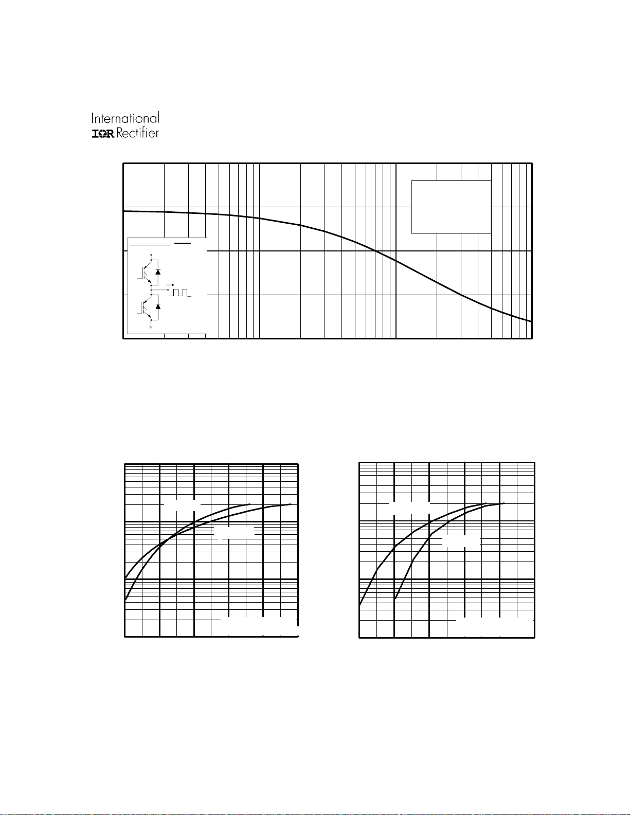
80
For both:
Duty cycle: 50%
T = 125°C
60
Square wave:
40
LOAD CURRENT (A)
20
0
0.1 1 10 100
60% of rated
v o l ta g e
I
Ideal diodes
f, Frequency (KHz
Fig. 1 - Typical Load Current vs. Frequency
(Load Current = I
of fundamental)
RMS
J
T = 9 0 °C
sink
Gate drive as specified
Po w e r Dis s ipa tion = W
58
1000
°
T = 25 C
J
100
T = 150 C
10
C
I , Collector Current (A)
Ic , Collector-to-Emitter Current (A)
1
1.0 1.5 2.0 2.5 3.0 3.5
V , Collector-to-Emitter Voltage (V)
CE
°
J
V = 15V
GE
80µs PULSE WIDTH
Fig. 2 - Typical Output Characteristics
1000
T = 150 C
100
10
C
I , Collector-to-Emitter Current (A)
1
5 6 7 8 9 10
V , Gate-to-Emitter Voltage (V)
GE
°
J
°
T = 25 C
J
V = 50V
CC
5µs PULSE WIDTH
Fig. 3 - Typical Transfer Characteristics
www.irf.com 3
 Loading...