

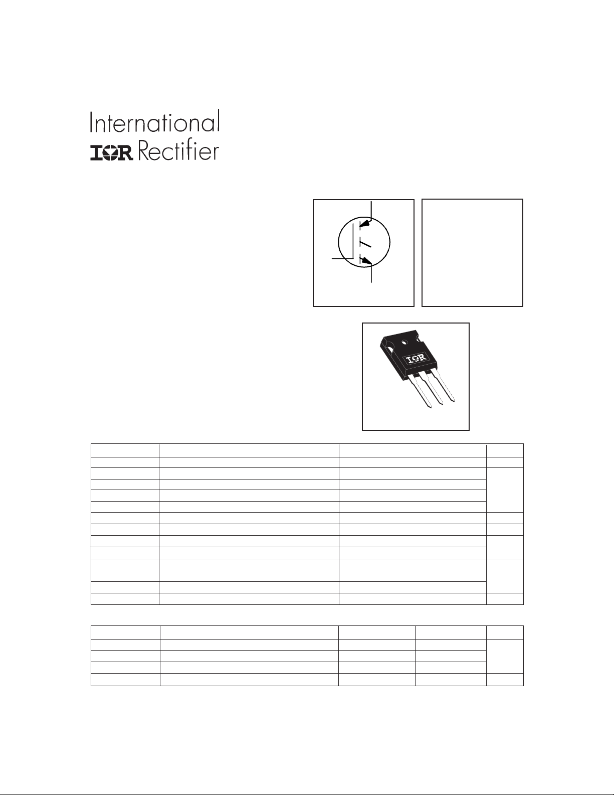
International Rectifier IRG4PH40U Datasheet
PD - 91612C
TO-247AC
IRG4PH40U
INSULATED GATE BIPOLAR TRANSISTOR
FeaturesFeatures
Features
FeaturesFeatures
C
Ultra Fast Speed IGBT
• UltraFast: Optimized for high operating
V
frequencies up to 40 kHz in hard switching,
= 1200V
CES
>200 kHz in resonant mode
• New IGBT design provides tighter
parameter distribution and higher efficiency than
previous generations
• Optimized for power conversion; SMPS, UPS
and welding
G
E
n-channel
V
CE(on) typ.
= 2.43V
@VGE = 15V, IC = 21A
• Industry standard TO-247AC package
Benefits
• Higher switching frequency capability than
competitive IGBTs
• Highest efficiency available
• Much lower conduction losses than MOSFETs
• More efficient than short circuit rated IGBTs
Absolute Maximum Ratings
Parameter Max. Units
V
CES
IC @ TC = 25°C Continuous Collector Current 41
IC @ TC = 100°C Continuous Collector Current 21 A
I
CM
I
LM
V
GE
E
ARV
PD @ TC = 25°C Maximum Power Dissipation 160
PD @ TC = 100°C Maximum Power Dissipation 65
T
J
T
STG
Collector-to-Emitter Breakdown Voltage 1200 V
Pulsed Collector Current Q 82
Clamped Inductive Load Current R 82
Gate-to-Emitter Voltage ± 20 V
Reverse Voltage Avalanche Energy S 270 mJ
Operating Junction and -55 to + 150
Storage Temperature Range
Soldering Temperature, for 10 seconds 300 (0.063 in. (1.6mm) from case )
Mounting torque, 6-32 or M3 screw. 10 lbf•in (1.1N•m)
W
°C
Thermal Resistance
Parameter Typ. Max. Units
R
θJC
R
θCS
R
θJA
Wt Weight 6 (0.21) ––– g (oz)
Junction-to-Case ––– 0.77
Case-to-Sink, Flat, Greased Surface 0.24 ––– °C/W
Junction-to-Ambient, typical socket mount ––– 40
www.irf.com 1
7/7/2000
IRG4PH40U
Electrical Characteristics @ TJ = 25°C (unless otherwise specified)
Parameter Min. Typ. Max. Units Conditions
V
(BR)CES
V
(BR)ECS
∆V
(BR)CES
V
CE(ON)
V
GE(th)
∆V
GE(th)
g
fe
I
CES
I
GES
Switching Characteristics @ TJ = 25°C (unless otherwise specified)
Q
g
Q
ge
Q
gc
t
d(on)
t
r
t
d(off)
t
f
E
on
E
off
E
ts
t
d(on)
t
r
t
d(off)
t
f
E
ts
L
E
C
ies
C
oes
C
res
Notes:
Collector-to-Emitter Breakdown Voltage 1200 —— VVGE = 0V, IC = 250µA
Emitter-to-Collector Breakdown Voltage T 18 —— VVGE = 0V, IC = 1.0A
/∆T
Temperature Coeff. of Breakdown Voltage — 0.43 — V/°CVGE = 0V, IC = 1.0mA
J
— 2.43 3.1 IC = 21A VGE = 15V
Collector-to-Emitter Saturation Voltage — 2.97 — IC = 41A See Fig.2, 5
— 2.47 — IC = 21A , TJ = 150°C
V
Gate Threshold Voltage 3.0 — 6.0 VCE = VGE, IC = 250µA
/∆TJTemperature Coeff. of Threshold Voltage — -11 — mV/°CVCE = VGE, IC = 250µA
Forward Transconductance U 16 24 — SVCE = 100V, IC = 21A
Zero Gate Voltage Collector Current
——250 VGE = 0V, VCE = 1200V
——2.0 µA VGE = 0V, VCE = 10V, TJ = 25°C
——5000 VGE = 0V, VCE = 1200V, TJ = 150°C
Gate-to-Emitter Leakage Current ——±100 nA VGE = ±20V
Parameter Min. Typ. Max. Units Conditions
Total Gate Charge (turn-on) — 86 130 IC = 21A
Gate - Emitter Charge (turn-on) — 13 20 nC VCC = 400V See Fig. 8
Gate - Collector Charge (turn-on) — 29 44 VGE = 15V
Turn-On Delay Time — 24 —
Rise Time — 24 — TJ = 25°C
Turn-Off Delay Time — 220 330 IC = 21A, VCC = 960V
ns
Fall Time — 180 270 VGE = 15V, RG = 10Ω
Turn-On Switching Loss — 1.04 — Energy losses include "tail"
Turn-Off Switching Loss — 3.40 — mJ See Fig. 9, 10, 14
Total Switching Loss — 4.44 5.2
Turn-On Delay Time — 24 — TJ = 150°C,
Rise Time — 25 — IC = 21A, VCC = 960V
Turn-Off Delay Time — 310 — VGE = 15V, RG = 10Ω
ns
Fall Time — 380 — Energy losses include "tail"
Total Switching Loss — 7.39 — mJ See Fig. 11, 14
Internal Emitter Inductance — 13 — nH Measured 5mm from package
Input Capacitance — 1800 — VGE = 0V
Output Capacitance — 120 — pF VCC = 30V See Fig. 7
Reverse Transfer Capacitance — 18 —ƒ = 1.0MHz
Q Repetitive rating; V
= 20V, pulse width limited by
GE
max. junction temperature. ( See fig. 13b )
R V
CC
(See fig. 13a)
= 80%(V
CES
), V
= 20V, L = 10µH, RG = 10Ω,
GE
T Pulse width ≤ 80µs; duty factor ≤ 0.1%.
U Pulse width 5.0µs, single shot.
S Repetitive rating; pulse width limited by maximum
junction temperature.
2 www.irf.com
IRG4PH40U
)
50
40
30
Square wave:
60% of rated
20
Load Current ( A )
10
0
0.1 1 10 100
voltag e
I
Ideal diodes
For both:
Duty cycle: 50%
T = 125°C
J
T = 90° C
sink
Gate drive as specified
Power D issipation = 35W
Triangular wave:
I
Clamp voltage:
80% of rated
f, Frequency (kHz
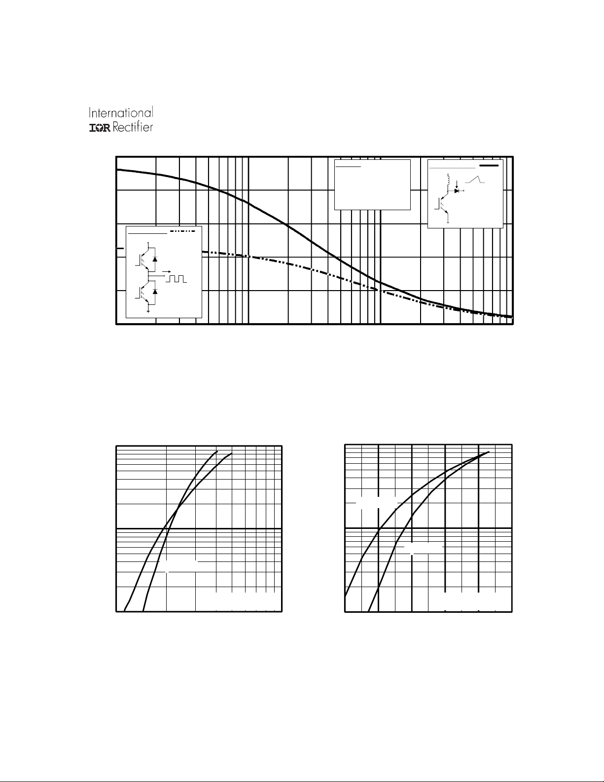
Fig. 1 - Typical Load Current vs. Frequency
(Load Current = I
of fundamental)
RMS
A
100
o
T = 150 C
J
10
o
T = 25 C
J
C
I , Collector-to-Emitter Current (A)
1
1 10
V , Collector-to-Emitter Voltage (V)
CE
V = 15V
GE
20µs PULSE WIDTH
100
o
T = 150 C
J
10
o
T = 25 C
J
C
I , Collector-to-Emitter Current (A)
1
5 6 7 8 9 10
V , Gate-to-Emitter Voltage (V)
GE
V = 50V
CC
5µs PULSE WIDTH
Fig. 2 - Typical Output Characteristics Fig. 3 - Typical Transfer Characteristics
www.irf.com 3
 Loading...