

International Rectifier IRG4PC50UD Datasheet
PD 91471B
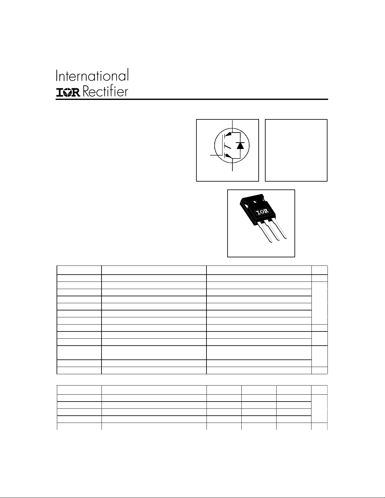
TO-247AC
IRG4PC50UD
INSULATED GATE BIPOLAR TRANSISTOR WITH
UltraFast CoPack IGBT
ULTRAFAST SOFT RECOVERY DIODE
FeaturesFeatures
Features
FeaturesFeatures
• UltraFast: Optimized for high operating
frequencies 8-40 kHz in hard switching, >200
kHz in resonant mode
• Generation 4 IGBT design provides tighter
parameter distribution and higher efficiency than
Generation 3
• IGBT co-packaged with HEXFRED
TM
ultrafast,
ultra-soft-recovery anti-parallel diodes for use in
G
n-channel
bridge configurations
• Industry standard TO-247AC package
Benefits
• Generation 4 IGBT's offer highest efficiencies
available
• IGBT's optimized for specific application conditions
• HEXFRED diodes optimized for performance with
IGBT's . Minimized recovery characteristics require
less/no snubbing
• Designed to be a "drop-in" replacement for equivalent
industry-standard Generation 3 IR IGBT's
Absolute Maximum Ratings
Parameter Max. Units
V
CES
IC @ TC = 25°C Continuous Collector Current 55
IC @ TC = 100°C Continuous Collector Current 27
I
CM
I
LM
IF @ TC = 100°C Diode Continuous Forward Current 25
I
FM
V
GE
PD @ TC = 25°C Maximum Power Dissipation 200
PD @ TC = 100°C Maximum Power Dissipation 78
T
J
T
STG
Collector-to-Emitter Voltage 600 V
Pulsed Collector Current Q 220 A
Clamped Inductive Load Current R 220
Diode Maximum Forward Current 220
Gate-to-Emitter Voltage ± 20 V
Operating Junction and -55 to +150
Storage Temperature Range °C
Soldering Temperature, for 10 sec. 300 (0.063 in. (1.6mm) from case)
Mounting Torque, 6-32 or M3 Screw. 10 lbf•in (1.1 N•m)
C
E
V
= 600V
CES
V
CE(on) typ.
= 1.65V
@VGE = 15V, IC = 27A
W
Thermal Resistance
Parameter Min. Typ. Max. Units
R
θJC
R
θJC
R
θCS
R
θJA
Wt Weight ------ 6 (0.21) ------ g (oz)
www.irf .com 1
Junction-to-Case - IGBT ------ ------ 0.64
Junction-to-Case - Diode ------ ------ 0.83 °C/W
Case-to-Sink, flat, greased surface ------ 0.24 -----Junction-to-Ambient, typical socket mount ----- ----- 40
12/30/00
IRG4PC50UD
Electrical Characteristics @ T
= 25°C (unless otherwise specified)
J
Parameter Min. Typ. Max. Units Conditions
V
(BR)CES
∆V
(BR)CES
V
CE(on)
Collector-to-Emitter Breakdown VoltageS 600 ---- ---- V VGE = 0V, IC = 250µA
/∆T
Temperature Coeff. of Breakdown Voltage ---- 0.60 ---- V/°CVGE = 0V, IC = 1.0mA
J
Collector-to-Emitter Saturation Voltage ---- 1.65 2.0 IC = 27A VGE = 15V
---- 2.0 ---- V IC = 55A See Fig. 2, 5
---- 1.6 ---- IC = 27A, TJ = 150°C
V
∆V
g
I
CES
V
fe
GE(th)
GE(th)
FM
Gate Threshold Voltage 3.0 ---- 6. 0 VCE = VGE, IC = 250µA
/∆TJTemperature Coeff. of Threshold Voltage ---- -13 ---- mV/°CVCE = VGE, IC = 250µA
Forward Transconductance T 16 24 ---- S VCE = 100V, IC = 27A
Zero Gate Voltage Collector Current ---- ---- 2 50 µA VGE = 0V, VCE = 600V
---- ---- 6500 V
= 0V, VCE = 600V, TJ = 150°C
GE
Diode Forward Voltage Drop ---- 1.3 1.7 V IC = 25A See Fig. 13
---- 1.2 1.5 IC = 25A, TJ = 150°C
I
GES
Gate-to-Emitter Leakage Current ---- ---- ±100 nA VGE = ±20V
Switching Characteristics @ TJ = 25°C (unless otherwise specified)
Parameter Min. Typ. Max. Units Conditions
Q
g
Qge Gate - Emitter Charge (turn-on) ---- 25 38 nC VCC = 400V See Fig. 8
Q
gc
t
d(on)
t
r
t
d(off)
t
f
E
on
E
off
E
ts
t
d(on)
t
r
t
d(off)
t
f
E
ts
L
E
C
ies
C
oes
C
res
t
rr
I
rr
Q
rr
di
(rec)M
2 www.irf.com
Total Gate Charge (turn-on) ---- 180 270 IC = 27A
Gate - Collector Charge (turn-on) ---- 61 90 VGE = 15V
Turn-On Delay Time ---- 46 ---- TJ = 25°C
Rise Time ---- 25 ---- n s IC = 27A, VCC = 480V
Turn-Off Delay Time ---- 140 230 VGE = 15V, RG = 5.0Ω
Fall Time ---- 74 110 Energy losses include "tail" and
Turn-On Switching Loss ---- 0.99 ---- diode reverse recovery.
Turn-Off Switching Loss ---- 0.59 ---- mJ See Fig. 9, 10, 11, 18
Total Switching Loss ---- 1.58 1.9
Turn-On Delay Time ---- 44 ---- TJ = 150°C, See Fig. 9, 10, 11, 18
Rise Time ---- 27 ---- n s IC = 27A, VCC = 480V
Turn-Off Delay Time ---- 240 ---- VGE = 15V, RG = 5.0Ω
Fall Time ---- 130 ---- Energy losses include "tail" and
Total Switching Loss ---- 2.3 ---- m J diode reverse recovery.
Internal Emitter Inductance ---- 13 ---- nH Measured 5mm from package
Input Capacitance ---- 4000 ---- VGE = 0V
Output Capacitance ---- 250 ---- pF VCC = 30V See Fig. 7
Reverse Transfer Capacitance ---- 52 ---- ƒ = 1.0MHz
Diode Reverse Recovery Time ---- 50 75 ns TJ = 25°C See Fig.
---- 105 160 TJ = 125°C 14 IF = 25A
Diode Peak Reverse Recovery Current ---- 4.5 10 A TJ = 25°C See Fig.
---- 8.0 15 TJ = 125°C 15 VR = 200V
Diode Reverse Recovery Charge ---- 112 375 nC TJ = 25°C See Fig.
---- 420 1200 TJ = 125°C 16 di/dt 200A/µs
/dt Diode Peak Rate of Fall of Recovery ---- 250 ---- A/µs TJ = 25°C
During t
b
---- 160 ---- TJ = 125°C
)
µ
)
40
A
30
IRG4PC50UD
Du ty cycle : 50%
T = 125 °C
J
T = 90 °C
sink
Gate drive as specified
Turn-on losses include
effec ts o f reve rs e re c ov e ry
Power Dissipation = 40W
20
60% of rated
volta g e
Load C urrent (A)
10
0
0.1 1 10 100
f, Frequency (kH z )
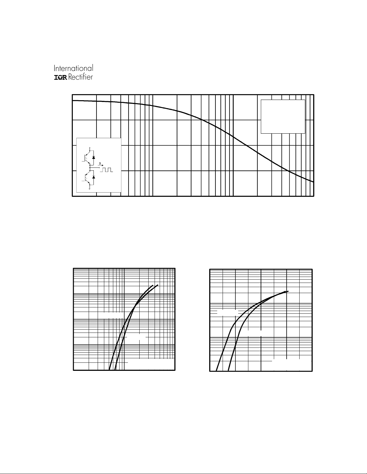
Fig. 1 - Typical Load Current vs. Frequency
1000
100
(Load Current = I
T = 150°C
10
J
of fundamental)
RMS
1000
100
T = 150°C
J
T = 25°C
T = 25°C
J
1
C
I , Collector-to-E m itter Curren t (A)
0.1
0110
V , Colle cto r-to-E mitter V o ltage (V
CE
V = 15V
GE
20
s PULSE WIDTH
A
Fig. 2 - Typical Output Characteristics
10
C
I , Colle cto r-to-E mitter C u rre nt (A)
1
4 6 8 10 12
V , G ate -to-Em itter V o ltage (V
GE
Fig. 3 - Typical Transfer Characteristics
J
V = 1 0V
CC
5µs PULSE WIDTH
A
www.irf .com 3
 Loading...