

International Rectifier IRG4PC50K Datasheet
PD - 91583B
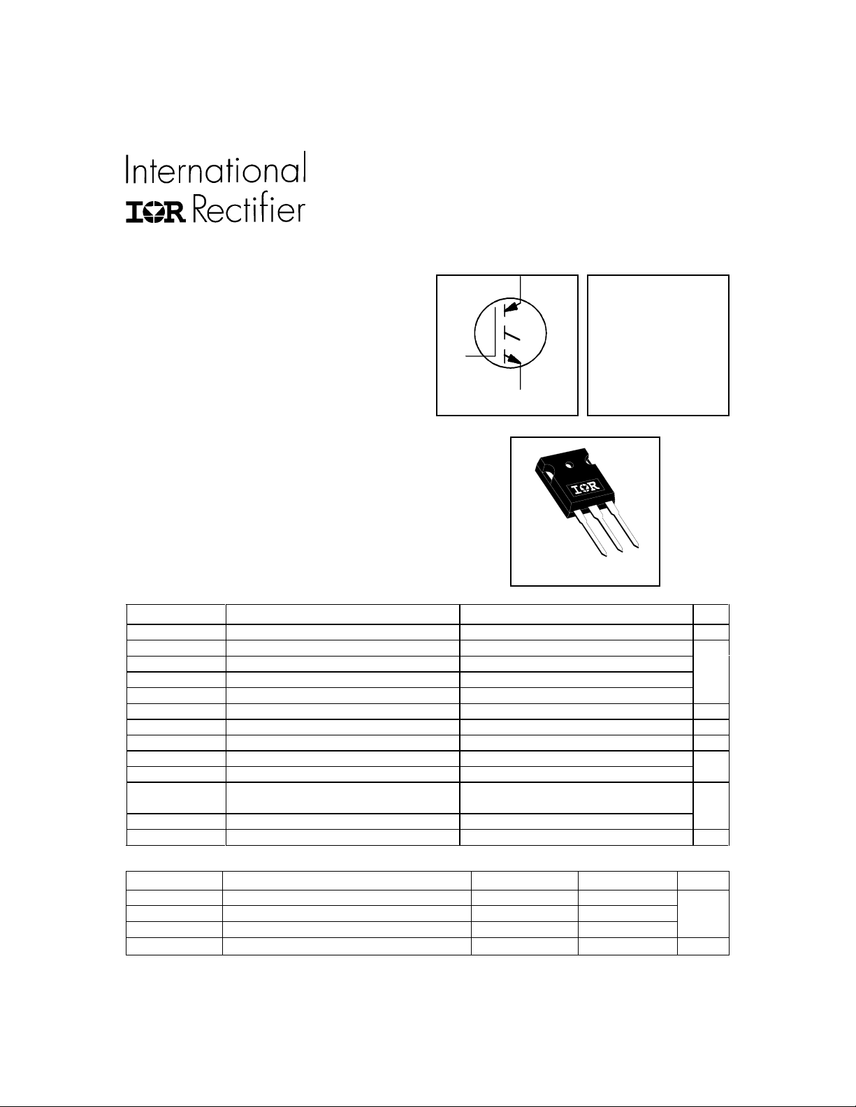
IRG4PC50K
INSULATED GATE BIPOLAR TRANSISTOR
FeaturesFeatures
Features
FeaturesFeatures
• High short circuit rating optimized for motor control,
=10µs, @360V VCE (start), TJ = 125°C,
t
sc
VGE = 15V
• Combines low conduction losses with high
switching speed
• Latest generation design provides tighter parameter
distribution and higher efficiency than previous
generations
G
n-channel
C
E
Benefits
• As a Freewheeling Diode we recommend our
HEXFRED
minimum EMI / Noise and switching losses in the
Diode and IGBT
• Latest generation 4 IGBTs offer highest power
density motor controls possible
• This part replaces the IRGPC50K and IRGPC50M
devices
TM
ultrafast, ultrasoft recovery diodes for
TO-247AC
Absolute Maximum Ratings
Parameter Max. Units
V
CES
IC @ TC = 25°C Continuous Collector Current 52
IC @ TC = 100°C Continuous Collector Current 30 A
I
CM
I
LM
t
sc
V
GE
E
ARV
PD @ TC = 25°C Maximum Power Dissipation 200 W
PD @ TC = 100°C Maximum Power Dissipation 78
T
J
T
STG
Collector-to-Emitter Voltage 600 V
Pulsed Collector Current Q 104
Clamped Inductive Load Current R 104
Short Circuit Withstand Time 10 µs
Gate-to-Emitter Voltage ±20 V
Reverse Voltage Avalanche Energy S 170 mJ
Operating Junction and -55 to +150
Storage Temperature Range °C
Soldering Temperature, for 10 sec. 300 (0.063 in. (1.6mm) from case)
Mounting torque, 6-32 or M3 screw. 10 lbf•in (1.1N•m)
Thermal Resistance
Parameter Typ. Max. Units
R
θJC
R
θCS
R
θJA
Wt Weight 6 (0.21) ––– g (oz)
Junction-to-Case ––– 0.64
Case-to-Sink, Flat, Greased Surface 0.24 ––– °C/W
Junction-to-Ambient, typical socket mount ––– 40
UltraFast IGBT
V
= 600V
CES
V
CE(on) typ.
@VGE = 15V, IC = 30A
= 1.84V
Short Circuit Rated
www.irf.com 1
4/15/2000
IRG4PC50K
Electrical Characteristics @ TJ = 25°C (unless otherwise specified)
Parameter Min. Typ. Max. Units Conditions
V
(BR)CES
V
(BR)ECS
∆V
(BR)CES
V
CE(ON)
V
GE(th)
∆V
GE(th)
g
fe
I
CES
I
GES
Switching Characteristics @ TJ = 25°C (unless otherwise specified)
Q
g
Q
ge
Q
gc
t
d(on)
t
r
t
d(off)
t
f
E
on
E
off
E
ts
t
sc
t
d(on)
t
r
t
d(off)
t
f
E
ts
L
E
C
ies
C
oes
C
res
Notes:
Q Repetitive rating; V
max. junction temperature. ( See fig. 13b )
R V
Collector-to-Emitter Breakdown Voltage 600 —— VVGE = 0V, IC = 250µA
Emitter-to-Collector Breakdown Voltage T 18 —— VVGE = 0V, IC = 1.0A
/∆T
Temperature Coeff. of Breakdown Voltage — 0.47 — V/°CVGE = 0V, IC = 1.0mA
J
— 1.84 2.2 I
Collector-to-Emitter Saturation Voltage — 2.19 — IC = 52 A See Fig.2, 5
— 1.79 — I
V
= 30A VGE = 15V
C
= 30A , TJ = 150°C
C
Gate Threshold Voltage 3.0 — 6.0 VCE = VGE, IC = 250µA
/∆TJTemperature Coeff. of Threshold Voltage — -12 — mV/°CVCE = VGE, IC = 250µA
Forward Transconductance U 17 24 — SVCE = 100 V, IC = 30A
Zero Gate Voltage Collector Current
——250 VGE = 0V, VCE = 600V
——2.0 VGE = 0V, VCE = 10V, TJ = 25°C
µA
——5000 VGE = 0V, VCE = 600V, TJ = 150°C
Gate-to-Emitter Leakage Current ——±100 nA VGE = ±20V
Parameter Min. Typ. Max. Units Conditions
Total Gate Charge (turn-on) — 200 300 IC = 30A
Gate - Emitter Charge (turn-on) — 25 38 nC VCC = 400V See Fig.8
Gate - Collector Charge (turn-on) — 85 130 VGE = 15V
Turn-On Delay Time — 38 —
Rise Time — 34 — TJ = 25°C
Turn-Off Delay Time — 160 240 IC = 30A, VCC = 480V
ns
Fall Time — 79 120 VGE = 15V, RG = 5.0Ω
Turn-On Switching Loss — 0.49 — Energy losses include "tail"
Turn-Off Switching Loss — 0.68 — mJ See Fig. 9,10,14
Total Switching Loss — 1.12 1.4
Short Circuit Withstand Time 10 —— µs VCC = 400V, TJ = 125°C
VGE = 15V, RG = 10Ω , V
Turn-On Delay Time — 37 — TJ = 150°C,
Rise Time — 35 — IC = 30A, VCC = 480V
Turn-Off Delay Time — 260 — VGE = 15V, RG = 5.0Ω
ns
Fall Time — 170 — Energy losses include "tail"
Total Switching Loss — 2.34 — mJ See Fig. 11,14
Internal Emitter Inductance — 13 — nH Measured 5mm from package
Input Capacitance — 3200 — VGE = 0V
Output Capacitance — 370 — pF VCC = 30V See Fig. 7
Reverse Transfer Capacitance — 95 —ƒ = 1.0MHz
= 80%(V
CC
CES
= 20V, pulse width limited by
GE
), V
= 20V, L = 10µH, RG = 5.0
GE
Ω
S Repetitive rating; pulse width limited by maximum
junction temperature.
T Pulse width ≤ 80µs; duty factor ≤ 0.1%.
U Pulse width 5.0µs, single shot.
CPK
< 500V
2 www.irf.com
IRG4PC50K
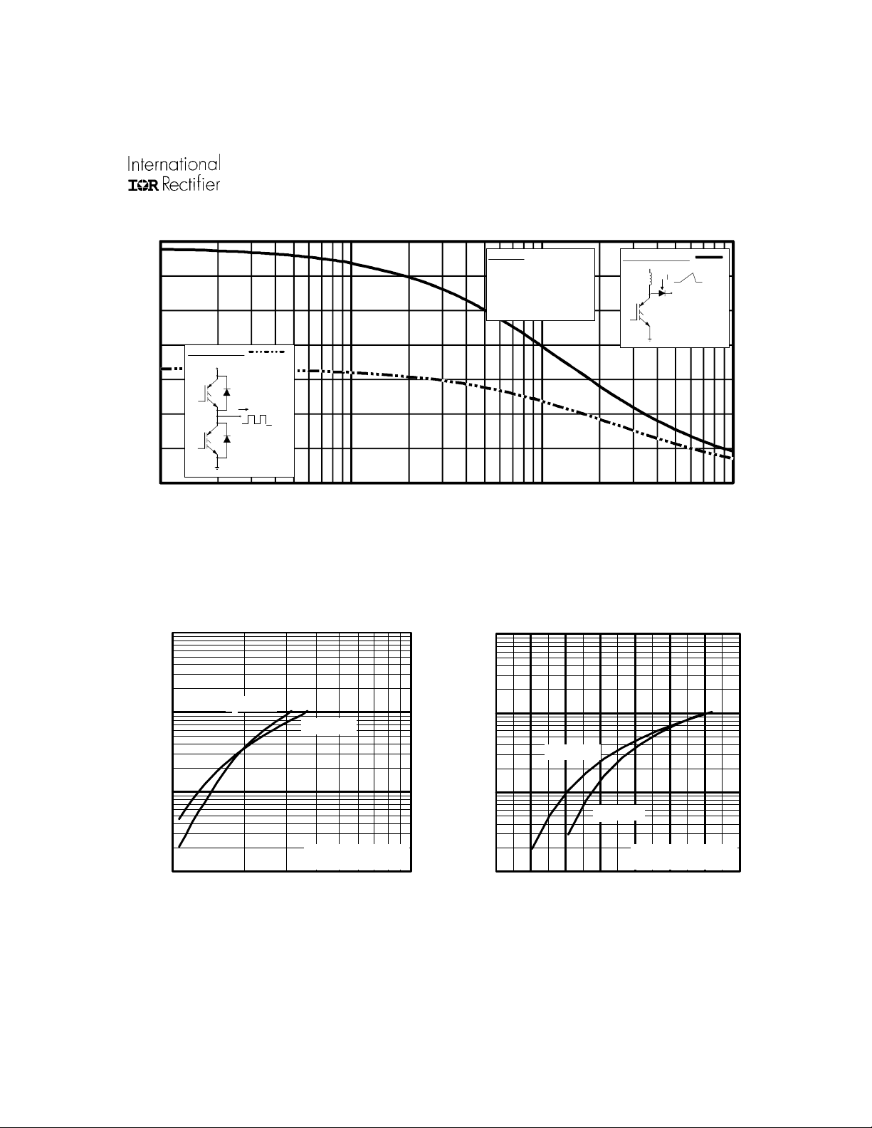
)
70
60
50
40
30
20
10
Square wave:
60% of rated
voltag e
I
Ideal diodes
0
0.1 1 10 100
For both:
Duty cy cle: 50%
T = 125°C
J
T = 90°C
sink
Gate drive as specified
Po w e r D i s s ip a t io n = 4 0 W
Triang ular wave:
Clamp v oltage:
80% of rated
f, Frequency (kHz
Fig. 1 - Typical Load Current vs. Frequency
(Load Current = I
1000
of fundamental)
RMS
1000
A
°
T = 25 C
100
10
C
I , Collector-to-Emitter Current (A)
1
1 10
J
°
T = 150 C
J
V = 15V
GE
20µs PULSE WIDTH
V , Collector-to-Emitter Voltage (V)
CE
100
T = 150 C
10
C
I , Collector-to-Emitter Current (A)
1
5 6 7 8 9 10 11 12
V , Gate-to-Emitter Voltage (V)
GE
°
J
°
T = 25 C
J
V = 50V
CC
5µs PULSE WIDTH
Fig. 2 - Typical Output Characteristics Fig. 3 - Typical Transfer Characteristics
www.irf.com 3
 Loading...