

International Rectifier IRG4BC30W-S Datasheet
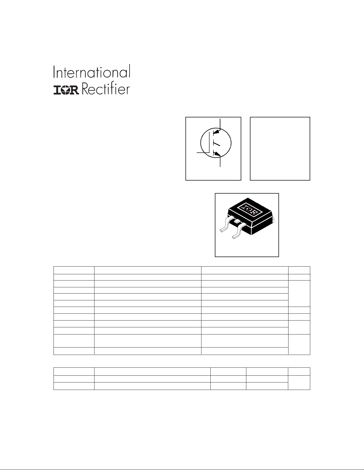
INSULATED GATE BIPOLAR TRANSISTOR
PD - 91790
IRG4BC30W-S
Features
• Designed expressly for Switch-Mode Power
Supply and PFC (power factor correction)
C
V
= 600V
CES
applications
• Industry-benchmark switching losses improve
efficiency of all power supply topologies
• 50% reduction of Eoff parameter
• Low IGBT conduction losses
• Latest-generation IGBT design and construction offers
G
E
n-channel
V
CE(on) typ.
= 2.10V
@VGE = 15V, IC = 12A
tighter parameters distribution, exceptional reliability
Benefits
• Lower switching losses allow more cost-effective
operation than power MOSFETs up to 150 kHz
("hard switched" mode)
• Of particular benefit to single-ended converters and
boost PFC topologies 150W and higher
• Low conduction losses and minimal minority-carrier
recombination make these an excellent option for
resonant mode switching as well (up to >>300 kHz)
2
D Pak
Absolute Maximum Ratings
Parameter Max. Units
V
CES
IC @ TC = 25°C Continuous Collector Current 23
IC @ TC = 100°C Continuous Collector Current 12 A
I
CM
I
LM
V
GE
E
ARV
PD @ TC = 25°C Maximum Power Dissipation 100
PD @ TC = 100°C Maximum Power Dissipation 42
T
J
T
STG
Collector-to-Emitter Breakdown Voltage 600 V
Pulsed Collector Current 92
Clamped Inductive Load Current 92
Gate-to-Emitter Voltage ± 20 V
Reverse Voltage Avalanche Energy 180 mJ
Operating Junction and -55 to + 150
Storage Temperature Range
Soldering Temperature, for 10 seconds 300 (0.063 in. (1.6mm from case )
W
°C
Thermal Resistance
Parameter Typ. Max. Units
R
θJC
R
θJA
Junction-to-Case ––– 1.2 °C/W
Junction-to-Ambient, ( PCB Mounted,steady-state)* ––– 40
* When mounted on 1" square PCB (FR-4 or G-10 Material ). For recommended footprint and soldering
techniques refer to application note #AN-994.
www.irf.com 1
8/13/98

IRG4BC30W-S
Electrical Characteristics @ TJ = 25°C (unless otherwise specified)
Parameter Min. Typ. Max. Units Conditions
V
(BR)CES
V
(BR)ECS
∆V
(BR)CES
V
CE(ON)
V
GE(th)
∆V
GE(th)
g
fe
I
CES
I
GES
Switching Characteristics @ TJ = 25°C (unless otherwise specified)
Q
g
Q
ge
Q
gc
t
d(on)
t
r
t
d(off)
t
f
E
on
E
off
E
ts
t
d(on)
t
r
t
d(off)
t
f
E
ts
L
E
C
ies
C
oes
C
res
Notes:
Collector-to-Emitter Breakdown Voltage 600 — — V VGE = 0V, IC = 250µA
Emitter-to-Collector Breakdown Voltage 18 — — V VGE = 0V, IC = 1.0A
/∆T
Temperature Coeff. of Breakdown Voltage — 0.34 — V/°C VGE = 0V, IC = 1.0mA
J
— 2.1 2.7 IC = 12A VGE = 15V
Collector-to-Emitter Saturation Voltage — 2.45 — IC = 23 A See Fig.2, 5
— 1.95 — IC = 12A , TJ = 150°C
V
Gate Threshold Voltage 3.0 — 6.0 VCE = VGE, IC = 250µA
/∆TJTemperature Coeff. of Threshold Voltage — -11 — mV/°C VCE = VGE, IC = 250µA
Forward Transconductance 11 16 — S VCE = 100 V, IC = 12A
Zero Gate Voltage Collector Current
— — 250 VGE = 0V, VCE = 600V
— — 2.0 VGE = 0V, VCE = 10V, TJ = 25°C
µA
— — 1000 VGE = 0V, VCE = 600V, TJ = 150°C
Gate-to-Emitter Leakage Current — — ±100 nA VGE = ±20V
Parameter Min. Typ. Max. Units Conditions
Total Gate Charge (turn-on) — 51 76 IC = 12A
Gate - Emitter Charge (turn-on) — 7.6 11 nC VCC = 400V See Fig.8
Gate - Collector Charge (turn-on) — 18 27 VGE = 15V
Turn-On Delay Time — 25 —
Rise Time — 16 — TJ = 25°C
Turn-Off Delay Time — 99 150 IC = 12A, VCC = 480V
ns
Fall Time — 67 100 VGE = 15V, RG = 23Ω
Turn-On Switching Loss — 0.13 — Energy losses include "tail"
Turn-Off Switching Loss — 0.13 — mJ See Fig. 9, 10, 13, 14
Total Switching Loss — 0.26 0.35
Turn-On Delay Time — 24 — TJ = 150°C,
Rise Time — 17 — IC = 12A, VCC = 480V
Turn-Off Delay Time — 150 — VGE = 15V, RG = 23Ω
ns
Fall Time — 150 — Energy losses include "tail"
Total Switching Loss — 0.55 — mJ See Fig. 11,13, 14
Internal Emitter Inductance — 7.5 — nH Measured 5mm from package
Input Capacitance — 980 — VGE = 0V
Output Capacitance — 71 — pF VCC = 30V See Fig. 7
Reverse Transfer Capacitance — 18 — ƒ = 1.0MHz
Repetitive rating; V
= 20V, pulse width limited by
GE
max. junction temperature. ( See fig. 13b )
V
CC
(See fig. 13a)
= 80%(V
CES
), V
= 20V, L = 10µH, RG = 23Ω,
GE
Pulse width ≤ 80µs; duty factor ≤ 0.1%.
Pulse width 5.0µs, single shot.
Repetitive rating; pulse width limited by maximum
junction temperature.
2 www.irf.com
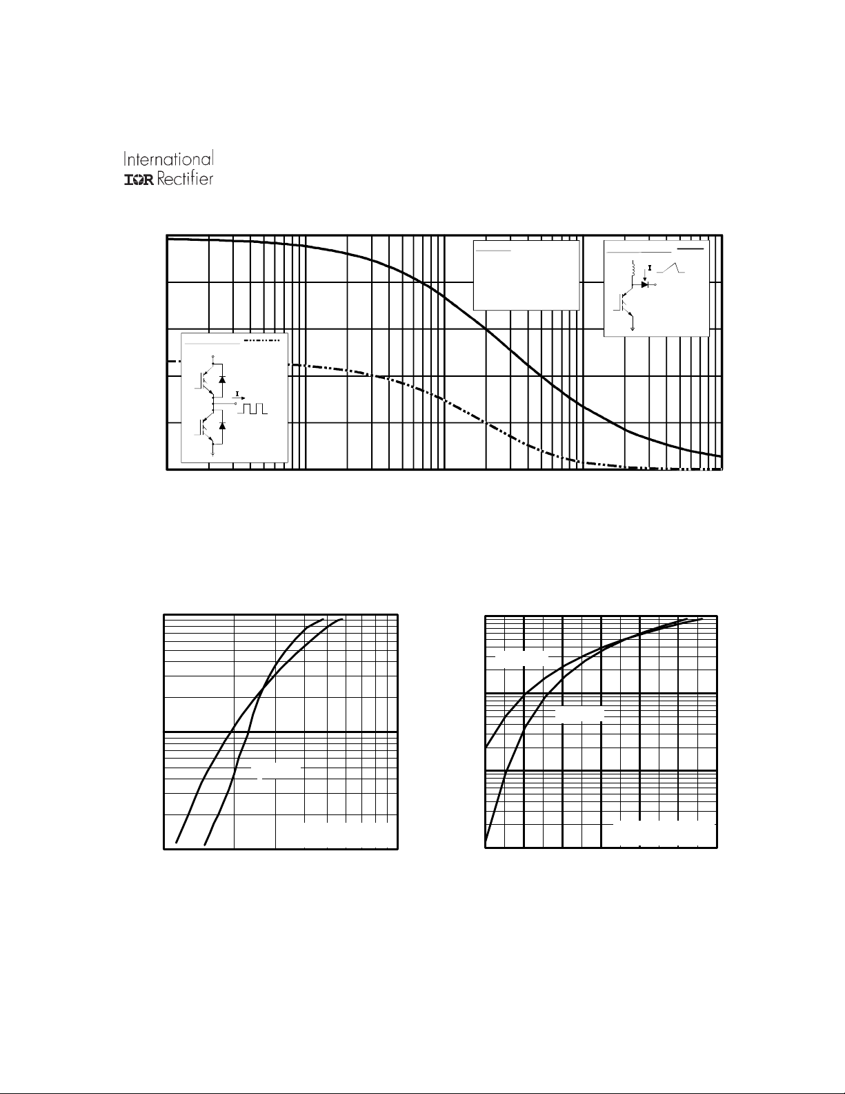
IRG4BC30W-S
A
5.0
4.0
3.0
2.0
Square wave:
60% of rated
voltage
For both:
Duty cycle: 50%
T = 125°C
J
T = 90°C
sink
Gate drive as specified
Power Dissipation = 1.75W
Triangular wave:
Clamp voltage:
80% of rated
Load C u rrent (A)
1.0
0.0
0.1 1 10 100 1000
Ideal diodes
f, Frequency (kHz)
Fig. 1 - Typical Load Current vs. Frequency
(For square wave, I=I
100
of fundamental; for triangular wave, I=IPK)
RMS
100
°
T = 150 C
J
10
T = 150 C
10
C
I , Collector-to-Emitter Current (A)
1
1 10
Fig. 2 - Typical Output Characteristics
°
J
°
T = 25 C
J
V = 15V
GE
20µs PULSE WIDTH
V , Collector-to-Emitter Voltage (V)
CE
°
T = 25 C
J
1
C
I , Collector-to-Emitter Current (A)
0.1
5.0 6.0 7.0 8.0 9.0 10.0 11.0
V , Gate-to-Emitter Voltage (V)
GE
V = 50V
CC
5µs PULSE WIDTH
Fig. 3 - Typical Transfer Characteristics
www.irf.com 3
 Loading...