

International Rectifier IRG4BC20SD-S Datasheet
PD -91794
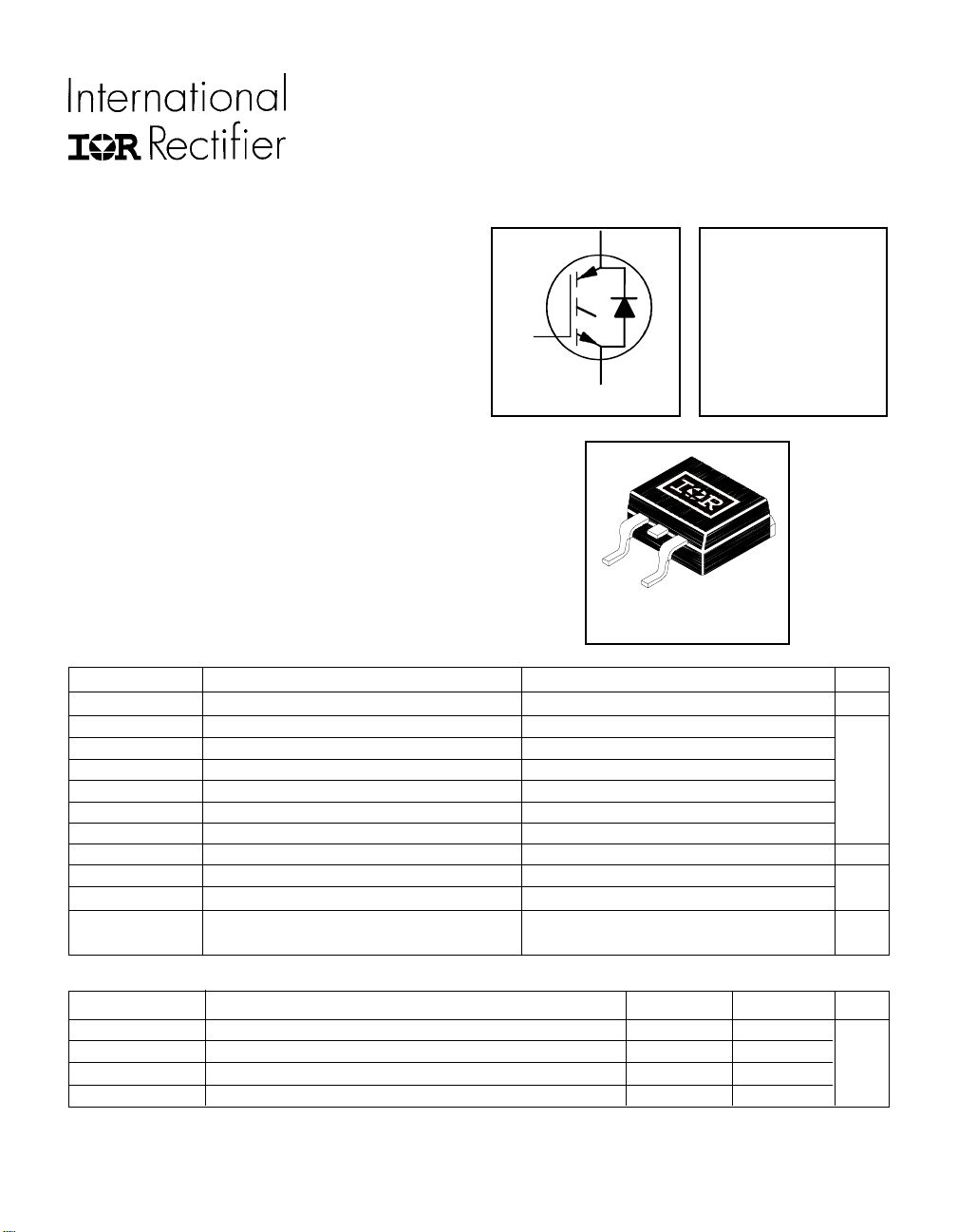
IRG4BC20SD-S
INSULATED GATE BIPOLAR TRANSISTOR WITH
Standard Speed IGBT
ULTRAFAST SOFT RECOVERY DIODE
FeaturesFeatures
Features
FeaturesFeatures
• Extremely low voltage drop 1.4Vtyp. @ 10A
• S-Series: Minimizes power dissipation at up to 3
KHz PWM frequency in inverter drives, up to 4
KHz in brushless DC drives.
• Very Tight Vce(on) distribution
• IGBT co-packaged with HEXFRED
TM
ultrafast,
G
ultra-soft-recovery anti-parallel diodes for use
in bridge configurations
• Industry standard D2Pak package
n-channel
Benefits
• Generation 4 IGBT's offer highest efficiencies
available
• IGBT's optimized for specific application conditions
• HEXFRED diodes optimized for performance with
IGBT's . Minimized recovery characteristics require
less/no snubbing
• Lower losses than MOSFET's conduction and
Diode losses
Absolute Maximum Ratings
Parameter Max. Units
V
CES
IC @ TC = 25°C Continuous Collector Current 19
IC @ TC = 100°C Continuous Collector Current 10
I
CM
I
LM
IF @ TC = 100°C Diode Continuous Forward Current 7.0
I
FM
V
GE
PD @ TC = 25°C Maximum Power Dissipation 60
PD @ TC = 100°C Maximum Power Dissipation 24
T
J
T
STG
Collector-to-Emitter Voltage 600 V
Pulsed Collector Current 38 A
Clamped Inductive Load Current 38
Diode Maximum Forward Current 38
Gate-to-Emitter Voltage ± 20 V
Operating Junction and -55 to +150
Storage Temperature Range °C
C
E
D Pak
V
= 600V
CES
V
CE(on) typ.
@VGE = 15V, IC = 10A
2
= 1.4V
W
Thermal Resistance
Parameter Typ. Max. Units
R
qJC
R
qJC
R
qJA
Wt Weight 1.44 ––– g (oz)
* When mounted on 1" square PCB (FR-4 or G-10 Material ). For recommended footprint and soldering techniques
refer to application note #AN-994.
www.irf.com 1
Junction-to-Case - IGBT ––– 2.1
Junction-to-Case - Diode ––– 3.5 °C/W
Junction-to-Ambient ( PCB Mounted,steady-state)* ––– 80
IRG4BC20SD-S
Electrical Characteristics @ T
= 25°C (unless otherwise specified)
J
Parameter Min. Typ. Max. Units Conditions
V
(BR)CES
DV
(BR)CES
V
CE(on)
Collector-to-Emitter Breakdown Voltageƒ 600 — — V VGE = 0V, IC = 250µA
/DT
Temperature Coeff. of Breakdown Voltage — 0.75 — V/°C VGE = 0V, IC = 1.0mA
J
Collector-to-Emitter Saturation Voltage — 1.40 1.6 IC = 10A VGE = 15V
— 1.85 — V IC = 19A See Fig. 2, 5
— 1.44 — IC = 10A, TJ = 150°C
V
DV
g
I
CES
GE(th)
GE(th)
fe
Gate Threshold Voltage 3.0 — 6.0 VCE = VGE, IC = 250µA
/DTJTemperature Coeff. of Threshold Voltage — -11 — mV/°C VCE = VGE, IC = 250µA
Forward Transconductance 2.0 5.8 — S VCE = 100V, IC = 10A
Zero Gate Voltage Collector Current — — 250 µA VGE = 0V, VCE = 600V
— — 1700 VGE = 0V, VCE = 600V, TJ = 150°C
V
FM
Diode Forward Voltage Drop — 1.4 1.7 V IC = 8.0A See Fig. 13
— 1.3 1.6 IC = 8.0A, TJ = 150°C
I
GES
Gate-to-Emitter Leakage Current — — ±100 nA VGE = ±20V
Switching Characteristics @ TJ = 25°C (unless otherwise specified)
Parameter Min. Typ. Max. Units Conditions
Q
g
Qge Gate - Emitter Charge (turn-on) — 4.3 6.5 nC VCC = 400V See Fig. 8
Q
gc
t
d(on)
t
r
t
d(off)
t
f
E
on
E
off
E
ts
t
d(on)
t
r
t
d(off)
t
f
E
ts
L
E
C
ies
C
oes
C
res
t
rr
I
rr
Q
rr
di
(rec)M
2 www.irf.com
Total Gate Charge (turn-on) — 27 40 IC = 10A
Gate - Collector Charge (turn-on) — 10 15 VGE = 15V
Turn-On Delay Time — 62 — TJ = 25°C
Rise Time — 32 — n s IC = 10A, VCC = 480V
Turn-Off Delay Time — 690 1040 VGE = 15V, RG = 50W
Fall Time — 480 730 Energy losses include "tail" and
Turn-On Switching Loss — 0.32 — diode reverse recovery.
Turn-Off Switching Loss — 2.58 — mJ See Fig. 9, 10, 11,18
Total Switching Loss — 2.90 4.5
Turn-On Delay Time — 64 — TJ = 150°C, See Fig. 10,11, 18
Rise Time — 35 — n s IC = 10A, VCC = 480V
Turn-Off Delay Time — 980 — VGE = 15V, RG = 50W
Fall Time — 800 — Energy losses include "tail" and
Total Switching Loss — 4.33 — mJ diode reverse recovery.
Internal Emitter Inductance — 7.5 — nH Measured 5mm from package
Input Capacitance — 550 — VGE = 0V
Output Capacitance — 39 — pF VCC = 30V See Fig. 7
Reverse Transfer Capacitance — 7.1 — ƒ = 1.0MHz
Diode Reverse Recovery Time — 37 55 ns TJ = 25°C See Fig.
—5590 TJ = 125°C 14 IF = 8.0A
Diode Peak Reverse Recovery Current — 3.5 5.0 A TJ = 25°C See Fig.
— 4.5 8.0 TJ = 125°C 15 VR = 200V
Diode Reverse Recovery Charge — 65 138 nC TJ = 25°C See Fig.
— 124 360 TJ = 125°C 16 di/dt = 200Aµs
/dt Diode Peak Rate of Fall of Recovery — 240 — A/µs TJ = 25°C See Fig.
During t
b
— 210 — TJ = 125°C 17
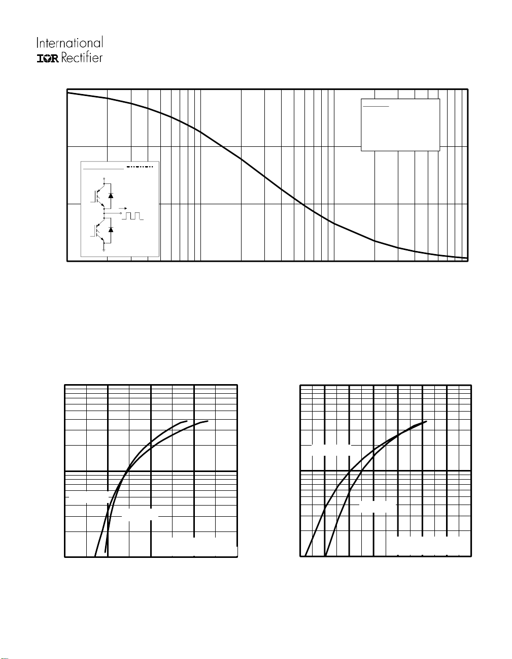
3.0
2.0
Square wave:
60% of rated
v o l ta g e
IRG4BC20SD-S
For both:
Duty cycle: 50%
T = 125°C
J
T = 9 0 °C
sink
Gate drive as specified
Po w e r Dis s ipa tion = W
1.7
1.0
I
LOAD CURRENT (A)
Ideal diodes
0.0
0.1 1 10 100
f, Frequency (KHz)
Fig. 1 - Typical Load Current vs. Frequency
100
10
T = 150 C
C
I , Collector Current (A)
°
J
T = 25 C
J
(Load Current = I
°
of fundamental)
RMS
100
10
T = 150 C
o
J
o
T = 25 C
J
V = 15V
GE
1
0.0 1.0 2.0 3.0 4.0
V , Collector-to-Emitter Voltage (V)
CE
20µs PULSE WIDTH
Fig. 2 - Typical Output Characteristics
I , Collector-to-Emitter Current (A)
1
5 6 7 8 9 10 11 12
V , Gate-to-Emitter Voltage (V)
GE
Fig. 3 - Typical Transfer Characteristics
V = 50V
CC
5µs PULSE WIDTH
C
www.irf.com 3
 Loading...