

International Rectifier IRG4BC15UD Datasheet
PD - 94082A
IRG4BC15UD
INSULATED GATE BIPOLAR TRANSISTOR WITH
UltraFast CoPack IGBT
ULTRAFAST SOFT RECOVERY DIODE
C
Features
• UltraFast: Optimized for high frequencies from10 to
30 kHz in hard switching
• IGBT Co-packaged with ultra-soft-recovery
antiparallel diode
• Industry standard TO-220AB package
G
E
V
= 600V
CES
V
CE(on) typ.
= 2.02V
@VGE = 15V, IC = 7.8A
n-channel
Benefits
• Best Value for Appliance and Industrial Applications
• High noise immune "Positive Only" gate drive Negative bias gate drive not necessary
• For Low EMI designs- requires little or no snubbing
• Single Package switch for bridge circuit applications
• Compatible with high voltage Gate Driver IC's
• Allows simpler gate drive
TO-220AB
Absolute Maximum Ratings
Parameter Max. Units
V
CES
IC @ TC = 25°C Continuous Collector Current 14
IC @ TC = 100°C Continuous Collector Current 7.8
I
CM
I
LM
IF @ TC = 100°C Diode Continuous Forward Current 4.0
I
FM
V
GE
PD @ TC = 25°C Maximum Power Dissipation 49
PD @ TC = 100°C Maximum Power Dissipation 19
T
J
T
STG
Collector-to-Emitter Voltage 600 V
Pulsed Collector Current 42 A
Clamped Inductive Load Current 42
Diode Maximum Forward Current 16
Gate-to-Emitter Voltage ± 20 V
W
Operating Junction and -55 to +150
Storage Temperature Range °C
Soldering Temperature, for 10 sec. 300 (0.063 in. (1.6mm) from case)
Mounting Torque, 6-32 or M3 Screw. 10 lbf•in (1.1 N•m)
Thermal Resistance
Parameter Min. Typ. Max. Units
R
θJC
R
θJC
R
θCS
R
θJA
Wt Weight ––– 2 (0.07) ––– g (oz)
www.irf.com 1
Junction-to-Case - IGBT ––– ––– 2.7
Junction-to-Case - Diode ––– ––– 7.0 °C/W
Case-to-Sink, flat, greased surface ––– 0.50 –––
Junction-to-Ambient, typical socket mount ––– ––– 80
03/20/01
IRG4BC15UD
Electrical Characteristics @ T
= 25°C (unless otherwise specified)
J
Parameter Min. Typ. Max. Units Conditions
V
(BR)CES
∆V
(BR)CES
V
CE(on)
Collector-to-Emitter Breakdown Voltage 600 ––– ––– V VGE = 0V, IC = 250µA
/∆T
Temperature Coeff. of Breakdown Voltage ––– 0.63 ––– V/°C VGE = 0V, IC = 1.0mA
J
Collector-to-Emitter Saturation Voltage ––– 2.02 2.4 IC = 7.8A VGE = 15V
––– 2.56 ––– V IC = 14A
––– 2.21 ––– IC = 7.8A, TJ = 150°C
V
∆V
g
I
fe
CES
GE(th)
GE(th)
Gate Threshold Voltage 3.0 ––– 6.0 VCE = VGE, IC = 250µA
/∆TJTemperature Coeff. of Threshold Voltage ––– -10 –– – mV/°C VCE = VGE, IC = 250µA
Forward Transconductance 4.1 6.2 ––– S VCE = 100V, IC = 7.8A
Zero Gate Voltage Collector Current ––– – –– 2 50 µA VGE = 0V, VCE = 600V
––– ––– 1400 VGE = 0V, VCE = 600V, TJ = 150°C
V
FM
Diode Forward Voltage Drop ––– 1.5 1.8 V IC = 4.0A
––– 1.4 1.7 IC = 4.0A, TJ = 150°C
I
GES
Gate-to-Emitter Leakage Current ––– ––– ±100 nA VGE = ±20V
Switching Characteristics @ TJ = 25°C (unless otherwise specified)
Parameter Min. Typ. Max. Units Conditions
Q
g
Qge Gate - Emitter Charge (turn-on) ––– 4.0 6.0 nC VCC = 400V
Q
gc
t
d(on)
t
r
t
d(off)
t
f
E
on
E
off
E
ts
t
d(on)
t
r
t
d(off)
t
f
E
ts
L
E
C
ies
C
oes
C
res
t
rr
I
rr
Q
rr
di
(rec)M
Total Gate Charge (turn-on) ––– 23 35 IC = 7.8A
Gate - Collector Charge (turn-on) ––– 9.6 14 VGE = 15V
Turn-On Delay Time ––– 17 ––– TJ = 25°C
Rise Time ––– 20 ––– ns IC = 7.8A, VCC = 480V
Turn-Off Delay Time ––– 160 240 VGE = 15V, RG = 75Ω
Fall Time ––– 83 120 Energy losses include "tail" and
Turn-On Switching Loss ––– 0.24 ––– diode reverse recovery.
Turn-Off Switching Loss ––– 0.26 ––– mJ
Total Switching Loss ––– 0.50 0.63
Turn-On Delay Time ––– 16 –– – TJ = 150°C,
Rise Time ––– 21 ––– ns IC = 7.8A, VCC = 480V
Turn-Off Delay Time ––– 180 ––– VGE = 15V, RG = 75Ω
Fall Time ––– 220 ––– Energy losses include "tail" and
Total Switching Loss ––– 0.76 ––– mJ diode reverse recovery.
Internal Emitter Inductance ––– 7.5 ––– nH Measured 5mm from package
Input Capacitance – –– 410 ––– VGE = 0V
Output Capacitance ––– 37 ––– pF VCC = 30V
Reverse Transfer Capacitance ––– 5.3 ––– ƒ = 1.0MHz
Diode Reverse Recovery Time ––– 28 42 ns TJ = 25°C
––– 38 57 TJ = 125°C IF = 4.0A
Diode Peak Reverse Recovery Current ––– 2.9 5. 2 A TJ = 25°C
––– 3.7 6.7 TJ = 125°C VR = 200V
Diode Reverse Recovery Charge ––– 40 60 nC TJ = 25°C
––– 70 110 TJ = 125°C di/dt 200A/µs
/dt Diode Peak Rate of Fall of Recovery ––– 280 ––– A/µs TJ = 25°C
During t
b
––– 240 ––– TJ = 125°C
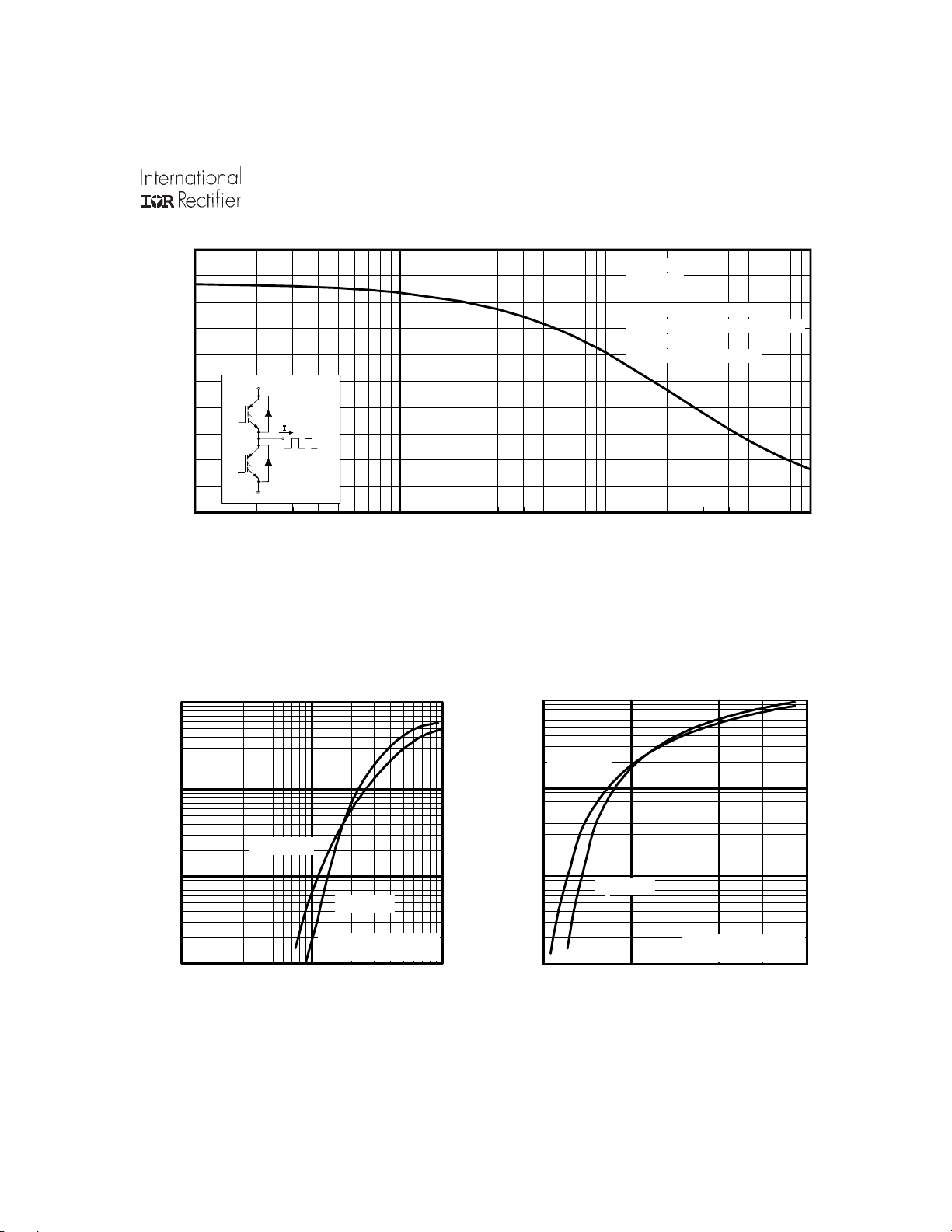
10
8
6
4
Load Current ( A )
60% o f ra te d
voltage
IRG4BC15UD
Duty cycle : 50%
Tj = 125°C
Tsink = 90°C
Gate drive as specified
Turn-on losses include effects of
reverse recovery
Power Dissipation = 11W
2
0
0.1 1 10 100
Ideal diodes
f , Frequency ( kHz )
Fig. 1 - Typical Load Current vs. Frequency
(Load Current = I
100
10
°
T = 150 C
J
1
°
T = 25 C
J
C
I , Collector-to-Emitter Current (A)
0.1
0.1 1 10
V , Collector-to-Emitter Voltage (V)
CE
V = 15V
GE
20µs PULSE WIDTH
of fundamental)
RMS
100
T = 150 C
10
1
C
I , Collector-to-Emitter Current (A)
0.1
5.0 10.0 15.0 20.0
°
J
T = 25 C
J
V , Gate-to-Emitter Voltage (V)
GE
°
V = 50V
CC
5µs PULSE WIDTH
Fig. 2 - Typical Output Characteristics Fig. 3 - Typical Transfer Characteristics
 Loading...