

International Rectifier IRFY9130CM Datasheet
HEXFET® PO WER MOSFET
Next Data SheetIndex
Previous Datasheet
To Order
Provisional Data Sheet No. PD 9.1293A
IRFY 9130CM
P-CHANNEL
-100 Volt, 0.3Ω HEXFET
International Rectifier’s HEXFET technology is the ke y to
its advanced line of power MOSFET tr ansistors. The efficient geometry design achieves very low on-state resistance combined with high transconductance.
HEXFET power MOSFETs also feature all of the wellestablished advantages of MOSFETs, such as voltage
control, very fast switching, ease of paralleling and electrical parameter temperature stability. They are well-suited
for applications such as switching power supplies, motor
controls, inverters, choppers, audio amplifiers, high energy pulse circuits, and virtually any application where
high reliability is required.
The HEXFET power MOSFET’ s totally isolated pac kage
eliminates the need for additional isolating material between
the device and the heatsink. This improves thermal efficiency and reduces drain capacitance.
Product Summary
Part Number BV
DSS
IRFY9130CM -100V 0.3Ω -11.2A
R
DS(on)
Features
n Hermetically Sealed
n Electrically Isolated
n Simple Drive Requirements
n Ease of Paralleling
Absolute Maximum Ratings
Parameter IRFY9130CM Units
ID @ VGS= -10V, TC = 25°C Continuous Drain Current -11.2
ID @ VGS= -10V, TC = 100°C Continuous Drain Current -7.1 A
I
DM
PD @ TC = 25°C Max. Pow er Dissipation 75 W
V
GS
E
AS
I
AR
E
AR
dv/dt Peak Diode Recover y dv/dt -5.5 V/ns
T
J
T
stg
Pulsed Drain Current -44
Linear Derating Factor 0.6 W/K
Gate-to-Source Voltage ±20 V
Single Pulse Avalance Energy 400 m J
Avalance Current -11.2 A
Repetitive Avalanche Energy 7.5 mJ
Operating Junction -55 to 150
Storage Temperature Range °C
Lead Temperature 300 (0.063 in (1.6mm) from case for 10 sec)
Weight 4.3(typical) g
I
D
IRFY9130CM Device
Next Data SheetIndex
Previous Datasheet
To Order
Electrical Characteristics @ Tj = 25°C (Unless Otherwise Specified)
Parameter Min Typ Max Units Test Conditions
BV
DSS
∆BV
DSS
R
DS(on)
V
GS(th)
g
fs
I
DSS
I
GSS
I
GSS
Q
g
Q
gs
Q
gd
t
d(on)
tr Rise Time — — 140 RG = 7.5Ω, VGS = -10V
t
d(off)
t
f
L
D
L
S
C
iss
C
oss
C
rss
Drain-to-Source Breakdown Voltage -100 — — V VGS = 0V, ID = -1.0mA
/∆TJTemperature Coefficient of Breakdown — -0.1 — V/°C Reference to 25°C, ID = -1.0mA
Voltage
Static Drain-to-Source — — 0.30 VGS = -10V, ID = -7.1A
On-State Resistance — — 0.35
Gate Threshold Voltage -2.0 — -4.0 V VDS = VGS, ID = -250µA
Forward Transconductance 2.5 — — S ( )VDS ≥ -15V, IDS = -7.1A
Zero Gate Voltage Drain Current — — -2 5
— — -250 VDS = 0.8 x max. rating
Ω
VGS = -10V, ID = -11.2A
Ω
V
= 0.8 x max. rating,VGS = 0V
DS
µA
VGS = 0V, TJ = 125°C
Gate-to-Source Leakage Forward — — -1 00 VGS = -20V
Gate-to-Source Leakage Reverse — — 100 VGS = 20V
nA
Total Gate Charge 14.7 — 30 VGS = -10V, ID = -11.2A
Gate-to-Source Charge 1.0 — 7.1 VDS = Max. Rating x 0.5
nC
Gate-to-Drain (‘Miller’) Charge 2.0 — 2.1 see figures 6 and 13
Turn-On Delay Time — — 60 VDD = -50V, ID = -11.2A
Turn-Off Delay Time — — 140
ns
Fall Time — — 140 see figure 10
Internal Drain Inductance — 8.7 —
Internal Source Inductance — 8.7 —
Measured from the drain
lead, 6mm (0.25 in.) from
package to center of die.
nH
Measured from the
source lead, 6mm (0.25
in.) from package to
source bonding pad.
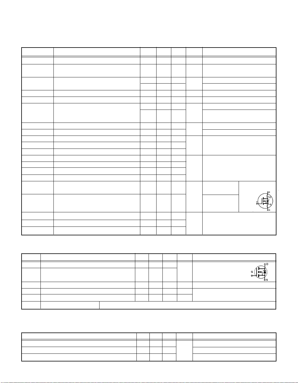
Modified MOSFET
showing the internal
inductances.
Input Capacitance — 800 — VGS = 0v, VDS = -25V
Output Capacitance — 350 — pF f = 1.0MHz.
Reverse Transfer Capacitance — 125 — see figure 5
symbol
Source-Drain Diode Ratings and Characteristics
Parameter Min Typ Max
I
Continuous Source Current (Body Diode) — — -11.2
S
I
Pulse Source Current (Body Diode) — — -44
SM
V
Diode Forward Voltage — — -4.7 V Tj = 25°C, IS = -11.2A, VGS = 0V
SD
t
Reverse Recovery Time — — 250 n s Tj = 25°C, IF = -11.2A, di/dt ≤ -100 A/µs
rr
Q
Reverse Recovery Charge — — 3.0 µC VDD ≤ -50 V
RR
t
Forward Turn-On Time
on
Intrinsic turn-on time is negligible. Turn-on speed is substantially controlled by LS + LD.
Thermal Resistance
Parameter Min Typ Max Units Test Conditions
R
Junction-to-Case — — 1.67
thJC
R
Junction-to-Ambient — — 80 K/W Typical socket mount
thJA
R
Case-to-Sink — 0.21 — Mounting surface flat, smooth
thCS
Units
Modified MOSFET
A
integr al reverse p-n junction rectifier.
Test Conditions
symbol showing the
 Loading...