

International Rectifier IRFP27N60K Datasheet
PD - 94407
SMPS MOSFET
Applications
l Hard Switching Primary or PFC Switch
l Switch Mode Power Supply (SMPS)
l Uninterruptible Power Supply
l High Speed Power Switching
l Motor Drive
V
DSS
600V 180mΩ 27A
IRFP27N60K
HEXFET® Power MOSFET
R
DS(on)
typ. I
Benefits
l Low Gate Charge Qg results in Simple
Drive Requirement
l Improved Gate, Avalanche and Dynamic
dv/dt Ruggedness
l Fully Characterized Capacitance and
Avalanche Voltage and Current
l Enhanced Body Diode dv/dt Capability
TO-247AC
Absolute Maximum Ratings
Parameter Max. Units
ID @ TC = 25°C Continuous Drain Current, VGS @ 10V 27
ID @ TC = 100°C Continuous Drain Current, VGS @ 10V 18 A
I
DM
PD @TC = 25°C Power Dissipation 500 W
V
GS
dv/dt Peak Diode Recovery dv/dt 13 V/ns
T
J
T
STG
Pulsed Drain Current 110
Linear Derating Factor 4.0 W/°C
Gate-to-Source Voltage ± 30 V
Operating Junction and -55 to + 150
Storage Temperature Range
Soldering Temperature, for 10 seconds 300
(1.6mm from case )
Mounting torqe, 6-32 or M3 screw 10 lbf•in (1.1N•m)
D
°C
Avalanche Characteristics
Symbol Parameter Typ. Max. Units
E
AS
I
AR
E
AR
Single Pulse Avalanche Energy ––– 530 mJ
Avalanche Current ––– 27 A
Repetitive Avalanche Energy ––– 50 mJ
Thermal Resistance
Symbol Parameter Typ. Max. Units
R
θJC
R
θCS
R
θJA
Junction-to-Case ––– 0.29
Case-to-Sink, Flat, Greased Surface 0.24 ––– °C/W
Junction-to-Ambient ––– 40
www.irf.com 1
03/20/02
IRFP27N60K
Static @ TJ = 25°C (unless otherwise specified)
Symbol Parameter Min. Typ. Max. Units Conditions
V
(BR)DSS
∆V
(BR)DSS
R
DS(on)
V
GS(th)
I
DSS
I
GSS
Dynamic @ TJ = 25°C (unless otherwise specified)
Symbol Parameter Min. Typ. Max. Units Conditions
g
fs
Q
g
Q
gs
Q
gd
t
d(on)
t
r
t
d(off)
t
f
C
iss
C
oss
C
rss
C
oss
C
oss
C
eff. Effective Output Capacitance ––– 250 ––– VGS = 0V, VDS = 0V to 480V
oss
Diode Characteristics
Symbol Parameter Min. Typ. Max. Units Conditions
I
S
I
SM
V
SD
t
rr
Q
rr
I
RRM
t
on
Drain-to-Source Breakdown Voltage 600 ––– ––– VVGS = 0V, ID = 250µA
/∆T
Breakdown Voltage Temp. Coefficient ––– 0.64 ––– V/°C Reference to 25°C, ID = 1mA
J
Static Drain-to-Source On-Resistance ––– 180 220 mΩ VGS = 10V, ID = 16A
Gate Threshold Voltage 3. 0 ––– 5.0 V VDS = VGS, ID = 250µA
Drain-to-Source Leakage Current
––– ––– 50
––– ––– 250 VDS = 480V, VGS = 0V, TJ = 125°C
Gate-to-Source Forward Leakage ––– ––– 100 V
Gate-to-Source Reverse Leakage ––– ––– -100
µA
nA
V
= 600V, VGS = 0V
DS
= 30V
GS
VGS = -30V
Forward Transconductance 14 ––– ––– SVDS = 50V, ID = 16A
Total Gate Charge ––– ––– 180 ID = 27A
Gate-to-Source Charge ––– ––– 56 nC VDS = 480V
Gate-to-Drain ("Miller") Charge ––– ––– 86 VGS = 10V, See Fig. 6 and 13
Turn-On Delay Time ––– 27 ––– VDD = 300V
Rise Time ––– 110 ––– ID = 27A
Turn-Off Delay Time ––– 43 ––– RG = 4.3Ω
ns
Fall Time ––– 38 ––– VGS = 10V,See Fig. 10
Input Capacitance ––– 4660 ––– VGS = 0V
Output Capacitance ––– 460 ––– VDS = 25V
Reverse Transfer Capacitance ––– 41 ––– pF ƒ = 1.0MHz, See Fig. 5
Output Capacitance ––– 5490 ––– VGS = 0V, VDS = 1.0V, ƒ = 1.0MHz
Output Capacitance ––– 120 ––– VGS = 0V, VDS = 480V, ƒ = 1.0MHz
Continuous Source Current MOSFET symbol
(Body Diode)
Pulsed Source Current integral reverse
(Body Diode)
––– –––
––– –––
27
110
showing the
A
p-n junction diode.
Diode Forward Voltage ––– ––– 1.5 V TJ = 25°C, IS = 27A, VGS = 0V
Reverse Recovery Time ––– 620 920 ns TJ = 25°C, IF = 27A
Reverse RecoveryCharge ––– 11 16 µC di/dt = 100A/µs
Reverse RecoveryCurrent ––– 36 53 A
Forward Turn-On Time Intrinsic turn-on time is negligible (turn-on is dominated by LS+LD)
D
G
S
Notes:
Repetitive rating; pulse width limited by
Pulse width ≤ 300µs; duty cycle ≤ 2%.
max. junction temperature. (See Fig. 11)
C
eff. is a fixed capacitance that gives the same charging time
Starting T
I
AS
I
SD
= 25°C, L = 1.4mH, RG = 25Ω,
J
= 27A, dv/dt = 13V/ns. (See Figure 12a)
≤ 27A, di/dt ≤ 390A/µs, V
DD
≤ V
(BR)DSS
,
oss
as C
oss
while V
is rising from 0 to 80% V
DS
DSS.
TJ ≤ 150°C.
2 www.irf.com
IRFP27N60K
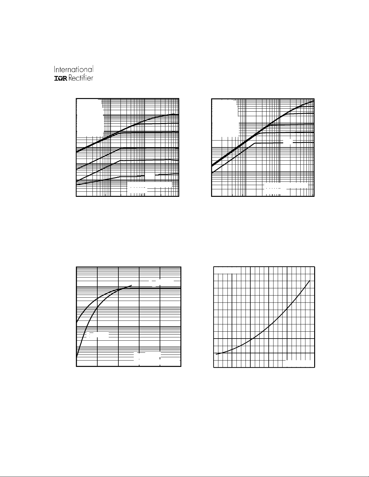
1000
100
10
1
0.1
, Drain-to-Source Current (A)
D
0.01
I
VGS
TOP 15V
12V
10V
8.0V
7.0V
6.0V
5.5V
BOTTOM 5.0V
20µs PULSE WIDTH
Tj = 25°C
0.001
0.1 1 10 100
VDS, Drain-to-Source Voltage (V)
1000.00
5.0V
100
10
1
0.1
, Drain-to-Source Current (A)
D
I
VGS
TOP 15V
12V
10V
8.0V
7.0V
6.0V
5.5V
BOTTOM 5.0V
20µs PULSE WIDTH
Tj = 150°C
0.01
0.1 1 10 100
VDS, Drain-to-Source Voltage (V)
Fig 2. Typical Output CharacteristicsFig 1. Typical Output Characteristics
3.5
28A
I =
D
5.0V
)
100.00
(Α
TJ = 150°C
10.00
1.00
TJ = 25°C
, Drain-to-Source Current
0.10
D
I
0.01
V
= 100V
DS
20µs PULSE WIDTH
5.0 7.0 9.0 11.0 13.0 15.0
VGS, Gate-to-Source Voltage (V)
Fig 3. Typical Transfer Characteristics
3.0
2.5
2.0
1.5
(Normalized)
1.0
0.5
DS(on)
R , Drain-to-Source On Resistance
0.0
-60 -40 -20 0 20 40 60 80 100 120 140 160
T , Junction Temperature ( C)
J
Fig 4. Normalized On-Resistance
V =
10V
GS
°
Vs. Temperature
www.irf.com 3
 Loading...