

International Rectifier IRFL4105 Datasheet
PD- 91381A
IRFL4105
HEXFET® Power MOSFET
l Surface Mount
l Advanced Process Technology
l Ultra Low On-Resistance
l Dynamic dv/dt Rating
l Fast Switching
l Fully Avalanche Rated
G
Description
Fifth Generation HEXFETs from International Rectifier
utilize advanced processing techniques to achieve
extremely low on-resistance per silicon area. This benefit,
combined with the fast switching speed and ruggedized
device design that HEXFET Power MOSFETs are well
known for, provides the designer with an extremely efficient
and reliable device for use in a wide variety of applications.
The SOT-223 package is designed for surface-mount
using vapor phase, infra red, or wave soldering techniques.
Its unique package design allows for easy automatic pickand-place as with other SOT or SOIC packages but has the
added advantage of improved thermal performance due to
an enlarged tab for heatsinking. Power dissipation of 1.0W
is possible in a typical surface mount application.
Absolute Maximum Ratings
Parameter Max. Units
ID @ TA = 25°C Continuous Drain Current, VGS @ 10V** 5.2
ID @ TA = 25°C Continuous Drain Current, VGS @ 10V* 3.7
ID @ TA = 70°C Continuous Drain Current, VGS @ 10V* 3.0
I
DM
PD @TA = 25°C Power Dissipation (PCB Mount)** 2.1 W
PD @TA = 25°C Power Dissipation (PCB Mount)* 1.0 W
V
GS
E
AS
I
AR
E
AR
dv/dt Peak Diode Recovery dv/dt 5.0 V/ns
T
J, TSTG
Pulsed Drain Current 30
Linear Derating Factor (PCB Mount)* 8.3 mW/°C
Gate-to-Source Voltage ± 20 V
Single Pulse Avalanche Energy 110 mJ
Avalanche Current 3.7 A
Repetitive Avalanche Energy 0.10 mJ
Junction and Storage Temperature Range -55 to + 150 °C
Thermal Resistance
Parameter Typ. Max. Units
R
θJA
R
θJA
* When mounted on FR-4 board using minimum recommended footprint.
** When mounted on 1 inch square copper board, for comparison with other SMD devices.
www.irf.com 1
Junction-to-Amb. (PCB Mount, steady state)* 90 120
Junction-to-Amb. (PCB Mount, steady state)** 50 60
D
R
DS(on)
V
DSS
= 55V
= 0.045Ω
ID = 3.7A
S
SOT -223
A
°C/W
1/14/99
IRFL4105
Electrical Characteristics @ TJ = 25°C (unless otherwise specified)
Parameter Min. Typ. Max. Units Conditions
V
(BR)DSS
∆V
(BR)DSS
R
DS(on)
V
GS(th)
g
fs
I
DSS
I
GSS
Q
g
Q
gs
Q
gd
t
d(on)
t
r
t
d(off)
t
f
C
iss
C
oss
C
rss
Drain-to-Source Breakdown Voltage 55 ––– ––– V VGS = 0V, ID = 250µA
/∆T
Breakdown Voltage Temp. Coefficient ––– 0.058 ––– V/°C Reference to 25°C, ID = 1mA
J
Static Drain-to-Source On-Resistance ––– ––– 0.045 Ω VGS = 10V, ID = 3.7A
Gate Threshold Voltage 2.0 ––– 4.0 V VDS = VGS, ID = 250µA
Forward Transconductance 3.8 ––– ––– S VDS = 25V, ID = 1.9A
Drain-to-Source Leakage Current
––– ––– 25
––– ––– 250 VDS = 44V, VGS = 0V, TJ = 150°C
Gate-to-Source Forward Leakage ––– ––– 100 VGS = 20V
Gate-to-Source Reverse Leakage ––– ––– -100
VDS = 55V, VGS = 0V
µA
nA
VGS = -20V
Total Gate Charge ––– 23 35 ID = 3.7A
Gate-to-Source Charge ––– 3. 4 5.1 nC VDS = 44V
Gate-to-Drain ("Miller") Charge ––– 9. 8 15 VGS = 10V, See Fig. 6 and 13
Turn-On Delay Time ––– 7.1 ––– VDD = 28V
Rise Time ––– 12 ––– ID = 3.7A
Turn-Off Delay Time ––– 19 ––– RG = 6.0Ω
ns
Fall Time ––– 12 ––– RD = 7.5Ω, See Fig. 10
Input Capacitance ––– 660 –– – VGS = 0V
Output Capacitance ––– 230 ––– pF VDS = 25V
Reverse Transfer Capacitance ––– 99 – –– ƒ = 1.0MHz, See Fig. 5
Source-Drain Ratings and Characteristics
Parameter Min. Typ. Max. Units Conditions
I
S
I
SM
V
SD
t
rr
Q
rr
Notes:
Repetitive rating; pulse width limited by
max. junction temperature. ( See fig. 11 )
V
DD
RG = 25Ω, I
2 www.irf.com
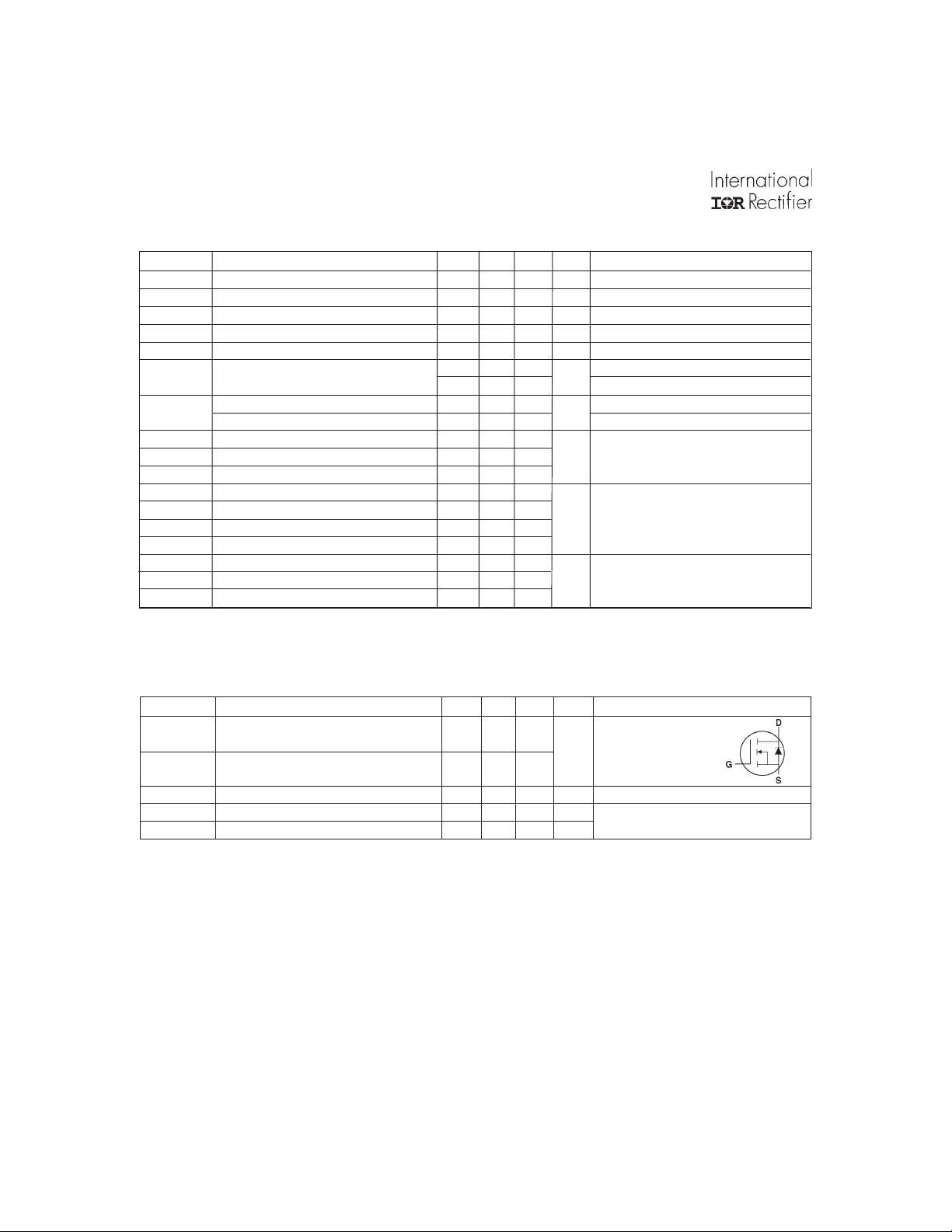
Continuous Source Current MOSFET symbol
(Body Diode) showing the
Pulsed Source Current integral reverse
(Body Diode) p-n junction diode.
––– –––
–––
–––
1.3
A
30
Diode Forward Voltage ––– ––– 1 .3 V TJ = 25°C, IS = 3.7A, VGS = 0V
Reverse Recovery Time ––– 55 82 ns TJ = 25°C, IF = 3.7A
Reverse RecoveryCharge –– – 120 170 nC di/dt = 100A/µs
I
≤ 3.7A, di/dt ≤ 110A/µs, V
SD
DD
≤ V
(BR)DSS
,
TJ ≤ 150°C
= 25V, starting TJ = 25°C, L = 16mH
= 3.7A. (See Figure 12)
AS
Pulse width ≤ 300µs; duty cycle ≤ 2%.
IRFL4105
)
A
)
A
A
A
100
V G S
TO P 1 5V
10 V
8. 0V
7. 0V
6. 0V
5. 5V
5. 0V
BOTTOM 4.5V
10
4.5V
D
I , D rain-to-Source C urrent (A)
20µs PUL SE WIDTH
T = 25°C
1
0.1 1 10 1 00
V , Dra in-t o- S o u rc e Vo ltage (V
DS
C
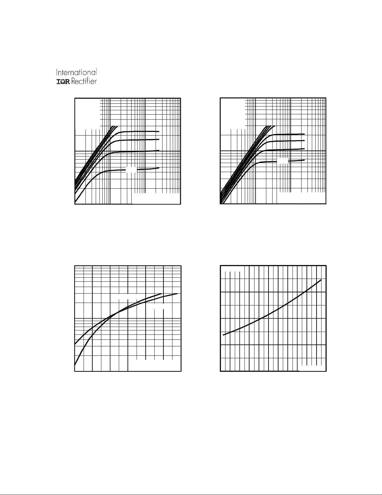
Fig 1. Typical Output Characteristics,
TJ = 25oC
100
100
VGS
TOP 15V
10V
8.0V
7.0V
6.0V
5.5V
5.0V
BOTTOM 4.5V
10
4.5V
D
I , Drain-to-Source Current (A)
20µs PULSE WIDTH
T = 150°C
1
0.1 1 10 1 00
V , Dra in-t o- S o u rc e Vo ltage (V
DS
J
Fig 2. Typical Output Characteristics,
TJ = 150oC
2.0
I = 3 . 7A
D
1.5
1.0
10
T = 25°C
J
T = 150°C
J
(No rm ali z e d )
0.5
D
I , Dra in-to-S o urc e C urre n t (A)
1
4.0 4.5 5.0 5.5 6.0 6.5 7.0
V , Gate -to-S o urce Vo ltag e (V)
GS
V = 25 V
DS
20µs PULSE WIDTH
Fig 3. Typical Transfer Characteristics
DS (on)
R , D r a in-to -S o u rc e O n R e s is ta nc e
0.0
-60 -40 -20 0 20 40 60 80 100 120 140 160
T , J unc tion T emp eratur e (°C )
J
Fig 4. Normalized On-Resistance
V = 1 0 V
GS
Vs. Temperature
www.irf.com 3
 Loading...