

International Rectifier IRFIZ48V Datasheet
PD-94072
IRFIZ48V
HEXFET® Power MOSFET
l Advanced Process Technology
l Ultra Low On-Resistance
l Isolated Package
l High Voltage Isolation = 2.5KVRMS
l Fast Switching
l Fully Avalanche Rated
l Optimized for SMPS Applications
G
Description
Advanced HEXFET® Power MOSFETs from International
Rectifier utilize advanced processing techniques to achieve
extremely low on-resistance per silicon area. This benefit,
combined with the fast switching speed and ruggedized
device design that HEXFET power MOSFETs are well
known for, provides the designer with an extremely efficient
and reliable device for use in a wide variety of applications.
The TO-220 Fullpak eliminates the need for additional
insulating hardware in commercial-industrial applications.
The moulding compound used provides a high isolation
capability and a low thermal resistance between the tab and
external heatsink. This isolation is equivalent to using a 100
micron mica barrier with standard TO-220 product. The
Fullpak is mounted to a heatsink using a single clip or by a
single screw fixing.
Absolute Maximum Ratings
Parameter Max. Units
ID @ TC = 25°C Continuous Drain Current, VGS @ 10V 39
ID @ TC = 100°C Continuous Drain Current, VGS @ 10V 27 A
I
DM
PD @TC = 25°C Power Dissipation 43 W
V
GS
I
AR
E
AR
dv/dt Peak Diode Recovery dv/dt 5.3 V/ns
T
J
T
STG
Pulsed Drain Current 290
Linear Derating Factor 0.29 W/°C
Gate-to-Source Voltage ± 20 V
Avalanche Current 72 A
Repetitive Avalanche Energy 15 mJ
Operating Junction and -55 to + 175
Storage Temperature Range
Soldering Temperature, for 10 seconds 300 (1.6mm from case )
Mounting torque, 6-32 or M3 srew 10 lbf•in (1.1N•m)
Thermal Resistance
Parameter Typ. Max. Units
R
θJC
R
θJA
Junction-to-Case ––– 3.5 °C/W
Junction-to-Ambient ––– 65
D
S
V
= 60V
DSS
R
= 12mΩ
DS(on)
= 39A
I
D
TO-220 FULLPAK
°C
www.irf.com 1
02/12/01
IRFIZ48V
Electrical Characteristics @ TJ = 25°C (unless otherwise specified)
Parameter Min. Typ. Max. Units Conditions
V
(BR)DSS
∆V
(BR)DSS
R
DS(on)
V
GS(th)
g
fs
I
DSS
I
GSS
Q
g
Q
gs
Q
gd
t
d(on)
t
r
t
d(off)
t
f
L
D
L
S
C
iss
C
oss
C
rss
E
as
Source-Drain Ratings and Characteristics
I
S
I
SM
V
SD
t
rr
Q
rr
t
on
Notes:
Repetitive rating; pulse width limited by
max. junction temperature. ( See fig. 11 )
Starting T
RG = 25Ω, I
I
SD
TJ ≤ 175°C
Pulse width ≤ 300µs; duty cycle ≤ 2%.
Drain-to-Source Breakdown Voltage 60 ––– ––– VVGS = 0V, ID = 250µA
/∆T
Breakdown Voltage Temp. Coefficient ––– 0.064 ––– V/°C Reference to 25°C, ID = 1mA
J
Static Drain-to-Source On-Resistance ––– ––– 12.0 mΩ VGS = 10V, ID = 43A
Gate Threshold Voltage 2.0 ––– 4.0 V VDS = VGS, ID = 250µA
Forward Transconductance 35 ––– ––– SVDS = 25V, ID = 43A
Drain-to-Source Leakage Current
––– ––– 25
––– ––– 250 VDS = 48V, VGS = 0V, TJ = 150°C
Gate-to-Source Forward Leakage ––– ––– 100 V
Gate-to-Source Reverse Leakage ––– ––– -100
VDS = 60V, VGS = 0V
µA
= 20V
GS
nA
VGS = -20V
Total Gate Charge ––– ––– 110 ID = 72A
Gate-to-Source Charge ––– ––– 29 nC VDS = 48V
Gate-to-Drain ("Miller") Charge ––– ––– 36 VGS = 10V, See Fig. 6 and 13
Turn-On Delay Time ––– 7.6 ––– VDD = 30V
Rise Time ––– 200 ––– ID = 72A
Turn-Off Delay Time ––– 157 ––– RG = 9.1Ω
ns
Fall Time ––– 166 ––– RD = 0.34Ω, See Fig. 10
4.5
Internal Drain Inductance
Internal Source Inductance ––– –––
––– –––
7.5
Between lead,
6mm (0.25in.)
nH
from package
and center of die contact
Input Capacitance ––– 1985 ––– VGS = 0V
Output Capacitance ––– 496 ––– VDS = 25V
Reverse Transfer Capacitance ––– 91 ––– pF ƒ = 1.0MHz, See Fig. 5
Single Pulse Avalanche Energy ––– 780 170 mJ IAS = 72A, L = 64mH
Parameter Min. Typ. Max. Units Conditions
Continuous Source Current MOSFET symbol
(Body Diode)
Pulsed Source Current integral reverse
(Body Diode)
––– –––
––– –––
39
290
showing the
A
p-n junction diode.
Diode Forward Voltage ––– ––– 2.0 V TJ = 25°C, IS = 72A, VGS = 0V
Reverse Recovery Time ––– 70 100 ns TJ = 25°C, IF = 72A
Reverse Recovery Charge ––– 155 233 nC di/dt = 100A/µs
Forward Turn-On Time Intrinsic turn-on time is negligible (turn-on is dominated by LS+LD)
This is a typical value at device destruction and represents
operation outside rated limits.
= 25°C, L = 64µH
J
= 72A. (See Figure 12)
AS
≤ 72A, di/dt ≤ 151A/µs, V
DD
≤ V
(BR)DSS
This is a calculated value limited to T
Uses IRFZ48V data and test conditions.
t = 60s, f = 60Hz
,
= 175°C .
J
D
G
S
D
G
S
2 www.irf.com
IRFIZ48V
)
1000
100
10
D
I , Drain-to-Source Current (A)
1
0.1 1 10 100
1000
VGS
TOP
15V
10V
8.0V
7.0V
6.0V
5.5V
5.0V
BOTTOM
4.5V
4.5V
20µs PULSE WIDTH
T = 25 C
J
V , Drain-to-Source Voltage (V)
DS
°
T = 25 C
J
°
1000
100
10
D
I , Drain-to-Source Current (A)
1
0.1 1 10 100
VGS
TOP
15V
10V
8.0V
7.0V
6.0V
5.5V
5.0V
BOTTOM
4.5V
4.5V
20µs PULSE WIDTH
T = 175 C
J
V , Drain-to-Source Voltage (V)
DS
°
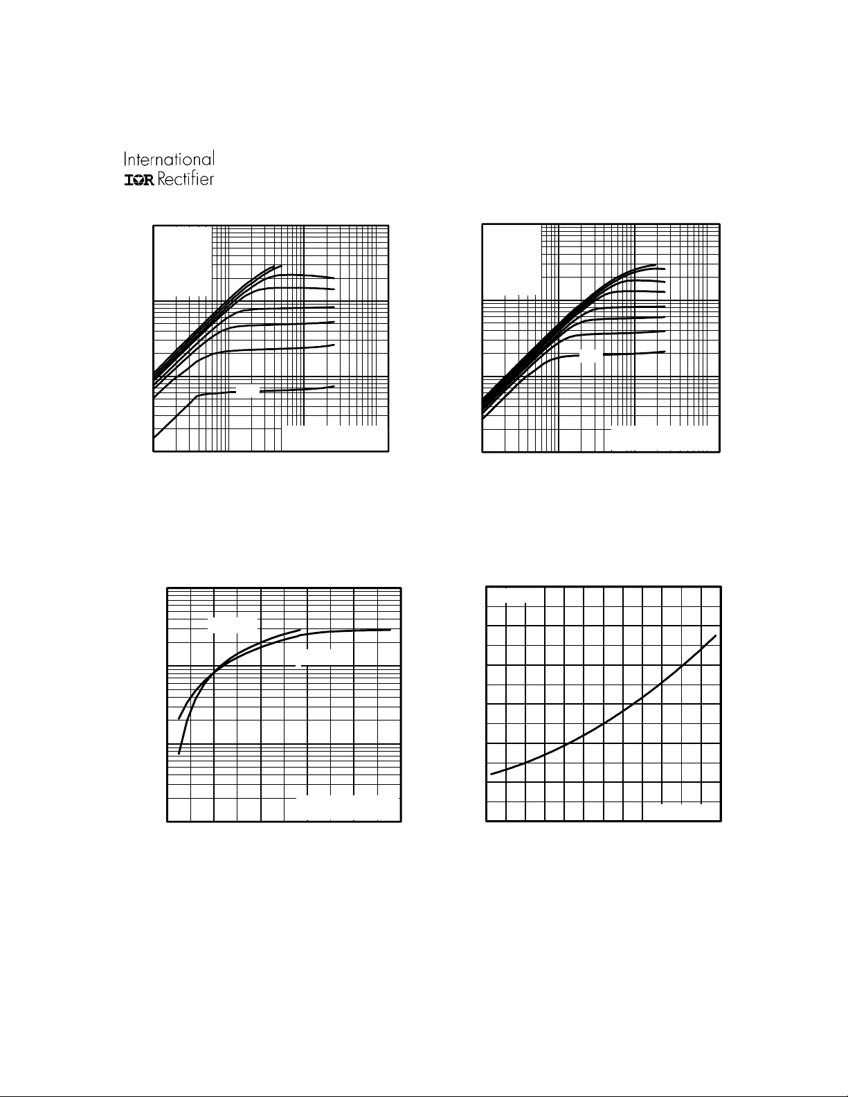
Fig 2. Typical Output CharacteristicsFig 1. Typical Output Characteristics
3.0
2.5
I =
D
72A
100
10
D
I , Drain-to-Source Current (A)
1
4 6 8 10 12 14
V , Gate-to-Source Voltage (V)
GS
T = 175 C
Fig 3. Typical Transfer Characteristics
°
J
V = 25V
DS
20µs PULSE WIDTH
2.0
1.5
(Normalized)
1.0
0.5
DS(on)
R , Drain-to-Source On Resistance
0.0
-60 -40 -20 0 20 40 60 80 100 120140 160 180
T , Junction Temperature( C
J
V =
Fig 4. Normalized On-Resistance
GS
°
10V
Vs. Temperature
www.irf.com 3
 Loading...