

International Rectifier IRFBA1404P Datasheet

PD - 93806
AUTOMOTIVE MOSFET
IRFBA1404P
Typical Applications
l Anti-lock Braking Systems (ABS)
l Electric Power Steering (EPS)
l Electric Braking
l Radiator Fan Control
Benefits
l Advanced Process Technology
l Ultra Low On-Resistance
l Increase Current Handling Capability
l 175°C Operating Temperature
l Fast Switching
l Dynamic dv/dt Rating
l Repetitive Avalanche Allowed up to Tjmax
G
Description
Specifically designed for Automotive applications, this Stripe Planar
design of HEXFET® Power MOSFETs utilizes the latest processing
techniques to achieve extremely low on-resistance per silicon area.
Additional features of this MOSFET are a 175oC junction operating
temperature, fast switching speed and improved ruggedness in
single and repetitive avalanche. The Super-220 TM is a package that
has been designed to have the same mechanical outline and pinout
as the industry standard TO-220 but can house a considerably
larger silicon die. The result is significantly increased current
handling capability over both the TO-220 and the much larger TO247 package. The combination of extremely low on-resistance
silicon and the Super-220 TM package makes it ideal to reduce the
component count in multiparalled TO-220 applications, reduce
system power dissipation, upgrade existing designs or have TO-247
performance in a TO-220 outline. This package has been designed
to meet automotive, Q101, qualification standard.
These benefits make this design an extremely efficient and reliable
device for use in Automotive applications and a wide variety of other
applications.
Absolute Maximum Ratings
Parameter Max. Units
ID @ TC = 25°C Continuous Drain Current, VGS @ 10V 206
ID @ TC = 100°C Continuous Drain Current, VGS @ 10V 145 A
I
DM
PD @TC = 25°C Power Dissipation 300 W
V
GS
E
AS
I
AR
E
AR
dv/dt Peak Diode Recovery dv/dt 5.0 V/ns
T
J
T
STG
Pulsed Drain Current 650
Linear Derating Factor 2.0 W/°C
Gate-to-Source Voltage ± 20 V
Single Pulse Avalanche Energy See Fig.12a, 12b, 15, 16 mJ
Avalanche Current A
Repetitive Avalanche Energy 30 mJ
Operating Junction and -40 to + 175
Storage Temperature Range -55 to + 175
Soldering Temperature, for 10 seconds 300 (1.6mm from case )
Recommended clip force 20 N
www.irf.com 1
HEXFET® Power MOSFET
D
R
DS(on)
V
DSS
= 40V
= 3.7mΩ
ID = 206A
S
Super-220™
°C
10/24/00
IRFBA1404P
Electrical Characteristics @ TJ = 25°C (unless otherwise specified)
Parameter Min. Typ. Max. Units Conditions
V
(BR)DSS
∆V
(BR)DSS
R
DS(on)
V
GS(th)
g
fs
I
DSS
I
GSS
Q
g
Q
gs
Q
gd
t
d(on)
t
r
t
d(off)
t
f
L
D
L
S
C
iss
C
oss
C
rss
C
oss
C
oss
C
eff. Effective Output Capacitance ––– 1540 ––– VGS = 0V, VDS = 0V to 32V
oss
Drain-to-Source Breakdown Voltage 40 –– – ––– V VGS = 0V, ID = 250µA
/∆T
Breakdown Voltage Temp. Coefficient ––– 0.036 ––– V/°C Reference to 25°C, ID = 1mA
J
Static Drain-to-Source On-Resistance ––– –– – 3.7 mΩ VGS = 10V, ID = 95A
Gate Threshold Voltage 2.0 ––– 4 .0 V VDS = 10V, ID = 250µA
Forward Transconductance 106 ––– ––– S VDS = 25V, ID = 60A
Drain-to-Source Leakage Current
––– ––– 20
––– ––– 250 VDS = 32V, VGS = 0V, TJ = 150°C
Gate-to-Source Forward Leakage ––– ––– 200 VGS = 20V
Gate-to-Source Reverse Leakage ––– ––– -200
VDS = 40V, VGS = 0V
µA
nA
VGS = -20V
Total Gate Charge ––– 1 60 200 ID = 95A
Gate-to-Source Charge ––– 35 ––– nC VDS = 32V
Gate-to-Drain ("Miller") Charge ––– 42 60 VGS = 10V
Turn-On Delay Time ––– 17 ––– VDD = 20V
Rise Time ––– 140 ––– ID = 95A
Turn-Off Delay Time ––– 72 ––– RG = 2.5Ω
ns
Fall Time ––– 26 ––– RD = 0.21Ω
Internal Drain Inductance
Internal Source Inductance ––– –––
––– –––
2.0
5.0
Between lead,
6mm (0.25in.)
nH
from package
and center of die contact
Input Capacitance ––– 7360 –– – VGS = 0V
Output Capacitance ––– 1680 – –– VDS = 25V
Reverse Transfer Capacitance ––– 240 ––– pF ƒ = 1.0MHz, See Fig. 5
Output Capacitance ––– 6630 – –– VGS = 0V, VDS = 1.0V, ƒ = 1.0MHz
Output Capacitance ––– 1490 – –– VGS = 0V, VDS = 32V, ƒ = 1.0MHz
D
G
S
Source-Drain Ratings and Characteristics
Parameter Min. Typ. Max. Units Conditions
I
S
I
SM
V
SD
t
rr
Q
rr
t
on
Continuous Source Current MOSFET symbol
(Body Diode)
Pulsed Source Current integral reverse
(Body Diode)
––– –––
––– –––
206
650
showing the
A
p-n junction diode.
G
Diode Forward Voltage ––– ––– 1.3 V TJ = 25°C, IS = 95A, VGS = 0V
Reverse Recovery Time ––– 71 110 ns TJ = 25°C, IF = 95A
Reverse Recovery Charge ––– 180 270 nC di/dt = 100A/µs
Forward Turn-On Time Intrinsic turn-on time is negligible (turn-on is dominated by LS+LD)
Thermal Resistance
Parameter Typ. Max. Units
R
θJC
R
θCS
R
θJA
Junction-to-Case ––– 0.50
Case-to-Sink, Flat, Greased Surface 0 .5 ––– °C/W
Junction-to-Ambient ––– 58
2 www.irf.com
D
S
IRFBA1404P
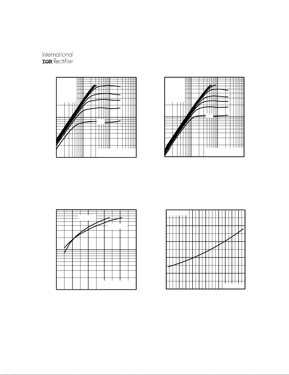
1000
100
D
I , Drain-to-Source Current (A)
10
0.1 1 10 100
1000
VGS
TOP
15V
10V
8.0V
7.0V
6.0V
5.5V
5.0V
BOTTOM
4.5V
4.5V
20µs PULSE WIDTH
T = 25 C
J
V , Drain-to-Source Voltage (V)
DS
°
T = 25 C
J
°
T = 175 C
J
1000
100
D
I , Drain-to-Source Current (A)
10
0.1 1 10 100
VGS
TOP
15V
10V
8.0V
7.0V
6.0V
5.5V
5.0V
BOTTOM
4.5V
4.5V
20µs PULSE WIDTH
T = 175 C
V , Drain-to-Source Voltage (V)
DS
°
J
Fig 2. Typical Output CharacteristicsFig 1. Typical Output Characteristics
2.5
°
2.0
159A
I =
D
1.5
100
1.0
(Normalized)
D
I , Drain-to-Source Current (A)
V = 25V
DS
10
4.0 5.0 6.0 7.0 8.0 9.0
V , Gate-to-Source Voltage (V)
GS
20µs PULSE WIDTH
Fig 3. Typical Transfer Characteristics
0.5
DS(on)
R , Drain-to-Source On Resistance
0.0
-60 -40 -20 0 20 40 60 80 100 120 140 160 180
T , Junction Temperature ( C)
J
Fig 4. Normalized On-Resistance
V =
10V
GS
°
Vs. Temperature
www.irf.com 3
 Loading...