

International Rectifier IRF7811A, IRF7809A Datasheet
A
PD - 93810
PD - 93811
IRF7809A/IRF7811A
IRF7809A/IRF7811A
PROVISIONAL DATASHEET
• N-Channel Application-Specific MOSFETs
• Ideal for CPU Core DC-DC Converters
• Low Conduction Losses
• Low Switching Losses
• Minimizes Parallel MOSFETs for high current
applications
Description
These new devices employ advanced HEXFET
®
Power
MOSFET technology to achieve an unprecedented balance
of on-resistance and gate charge. The reduced conduction
and switching losses make them ideal for high efficiency
DC-DC converters that power the latest generation of
microprocessors.
Both the IRF7809A and IRF7811A have been optimized
and are 100% tested for all parameters that are critical in
synchronous buck converters including R
and Cdv/dt-induced turn-on immunity . The IRF7809A offers
particulary low R
synchronous FET applications. The IRF7811A offers an
and high Cdv/dt immunity for
DS(on)
extremely low combination of Qsw & R
losses in control FET applications.
, gate charge
DS(on)
for reduced
DS(on)
The package is designed for vapor phase, infra-red,
convection, or wave soldering techniques. Power
dissipation of greater than 2W is possible in a typical PCB
mount application.
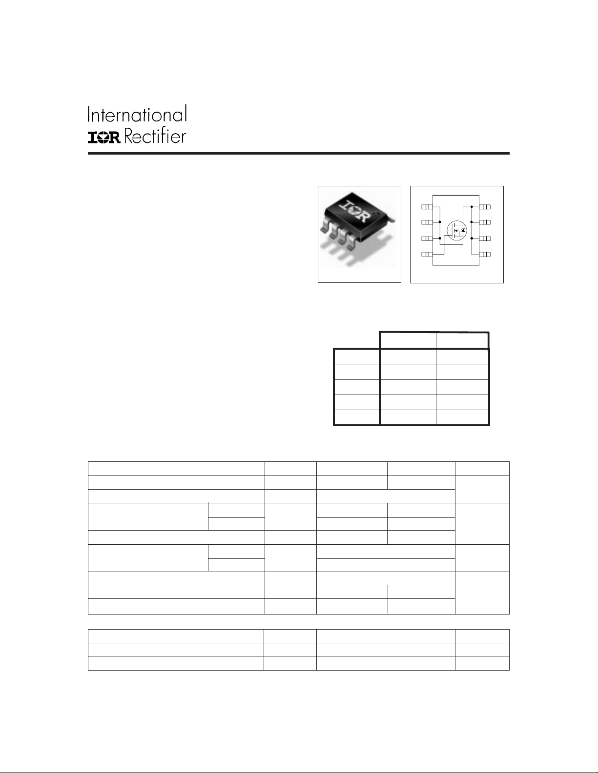
HEXFET® Chipset for DC-DC Converters
1
S
2
S
3
S
4
SO-8
DEVICE RATINGS
IRF7809A IRF7811A
V
DS
R
(on)
DS
Q
G
Q
sw
Q
oss
30V 28V
8.5 mΩ 12 mΩ
73 nC 23 n C
22.5 nC 7 n C
30 nC 31 n C
Top View
A
8
D
7
D
6
D
5
DG
Absolute Maximum Ratings
Parameter Symbol IRF7809A IRF7811A Units
Drain-Source Voltage V
Gate-Source V oltage V
Continuous Drain or Source T
Current (V
≥ 4.5V) TL = 90°C 14.2 11.2 A
GS
= 25°C I
A
Pulsed Drain Current I
Power Dissipation T
Junction & Storage Temperature Range T
= 25°C P
A
T
= 90°C 2.4
L
J, TSTG
Continuous Source Current (Body Diode) I
Pulsed Source Current I
DS
GS
D
DM
D
S
SM
30 28 V
±12
14.5 11.4
100 100
2.5 W
–55 to 150 °C
2.5 2.5 A
50 50
Thermal Resistance
Parameter Max. Units
Maximum Junction-to-Ambient R
Maximum Junction-to-Lead R
θJA
θJL
50 °C/W
25 °C/W
www.irf.com 1
01/19/00

IRF7809A/IRF7811A
Electrical Characteristics
IRF7809A IRF7811A
Parameter Min Typ Max Min Typ Max Units Conditions
Drain-to-Source BV
Breakdown Voltage*
Static Drain-Source R
on Resistance*
Gate Threshold Voltage* V
Drain-Source Leakage I
Current*
Current* 150 150 V
DSS
30 – – 28 – – V VGS = 0V, ID = 250µA
DSS
DS
GS(th)
(on)
7 8. 5 10 12 mΩ VGS = 4.5V, ID = 15A
1.0 1.0 V VDS = VGS,ID = 250µA
30 30 µA VDS = 24V, VGS = 0
DS
= 24V, VGS = 0,
Tj = 100°C
Gate-Source Leakage I
Current*
Total Gate Chg Cont FET* Q
Total Gate Chg Sync FET* Q
Pre-Vth Q
Gate-Source Charge
Post-Vth Q
Gate-Source Charge
Gate to Drain Charge Q
Switch Chg(Q
+ Qgd)* Q
gs2
Output Charge* Q
Gate Resistance R
Turn-on Delay Time t
Rise Time t
Turn-off Delay Time td
Fall Time t
Input Capacitance C
Output Capacitance C
Reverse Transfer Capacitance C
GSS
d (on)
r
f
iss
oss
G
G
GS1
GS2
GD
sw
oss
G
(off)
– 7300 – – 1800 –
– 900 – – 900 – pF VDS = 16V, VGS = 0
– 350 – – 60 –
rss
±100 ±100 nA VGS = ±12V
61 75 19 23 VGS=5V , ID=15A, VDS=16V
55 73 17 20.5 VGS = 5V, VDS< 100mV
14 2.7 VDS = 16V, ID = 15A
3.5 1.3 nC
13.5 4.5
17 22.5 5.8 7.0
25 30 26 31 VDS = 16V, VGS = 0
1.1 1.8 Ω
19 8 VDD = 16V, ID = 15A
94nsV
GS
= 5V
32 16 Clamped Inductive Load
12 8
Source-Drain Rating & Characteristics
Parameter Min Typ Max Min Typ Max Units Conditions
Diode Forward V
Voltage*
Reverse Recovery Q
Charge
Reverse Recovery Q
SD
rr
rr(s)
Charge (with Parallel (with 10BQ040)
Schottky) VDS = 16V, VGS = 0V, IS = 15A
1.0 1.0 V IS = 15A, VGS = 0V
94 82 nC di/dt ~ 700A/µs
VDS = 16V, VGS = 0V, IS = 15A
87 74 di/dt = 700A/µs
Notes:
Repetitive rating; pulse width limited by max. junction temperature.
Pulse width ≤ 300 µs; duty cycle ≤ 2%.
When mounted on 1 inch square copper board, t < 10 sec.
Typ = measured - Q
* Devices are 100% tested to these parameters.
oss
www.irf.com2
 Loading...